
Power switch circuit sizing technique

a power switch and circuit technology, applied in pulse technique, semiconductor/solid-state device details, instruments, etc., can solve the problems of complex cooling solutions, increased performance, and need for more expensive packaging

Inactive Publication Date: 2005-08-02
GLOBALFOUNDRIES US INC
View PDF7 Cites 8 Cited by
  • Summary
  • Abstract
  • Description
  • Claims
  • Application Information

AI Technical Summary

Benefits of technology

[0017]FIG. 8 is a flowchart showing how the invention matches the

Problems solved by technology

This increasing power density in turn drives the need for more expensive packaging, complex cooling solutions and decreased reliability due to increased temperatures.
Therefore, there is a need for a method and structure that increases performance, while at the same time decreases power consumption.

Method used


Image

  • Power switch circuit sizing technique
  • Power switch circuit sizing technique
  • Power switch circuit sizing technique

Examples


Embodiment Construction

[0018]The power challenges posed by advanced technologies force system designers to make choices concerning devices, structures and voltage levels for the functions they are designing. In previous generations, large functional blocks were not integrated on the same chip, so these choices could be made independently for each block. High levels of integration supported by system-on-a-chip (SoC) enabling technology drive single chip implementations, where traditional approaches to power distribution and performance optimization fail to provide the flexibility of voltage and technology optimization of the previously disintegrated solution.

[0019]Newer technologies divide each semiconductor chip into individual functional blocks (voltage islands) as explained in copending U.S. patent application Ser. Nos. 10 / 065,201 and 10 / 065,202 both of which are hereby incorporated by reference. These voltage islands of the SoC design can have power characteristics unique from the rest of the design an...


PUM


Abstract

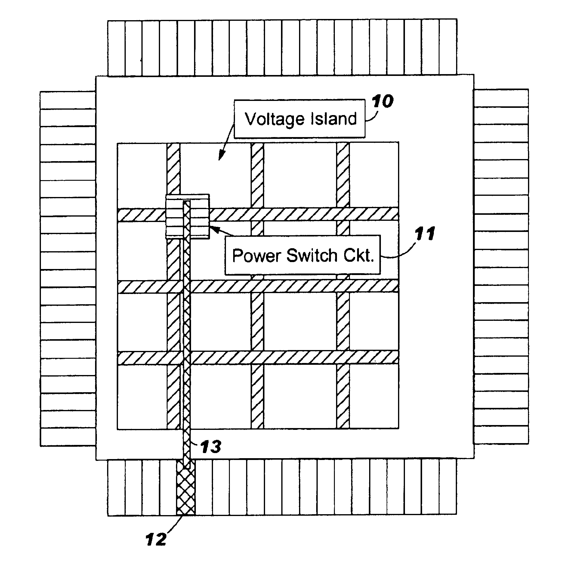
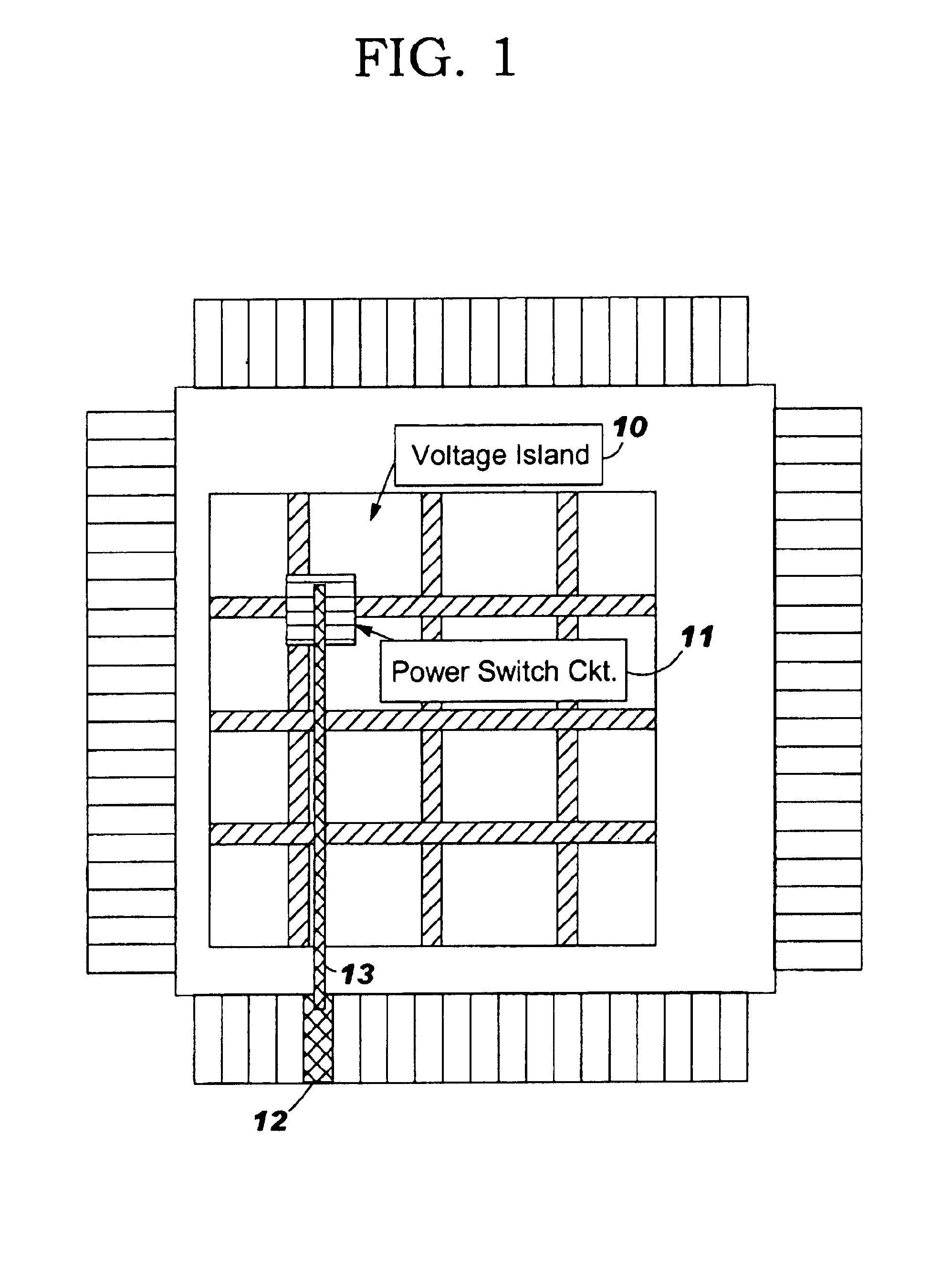
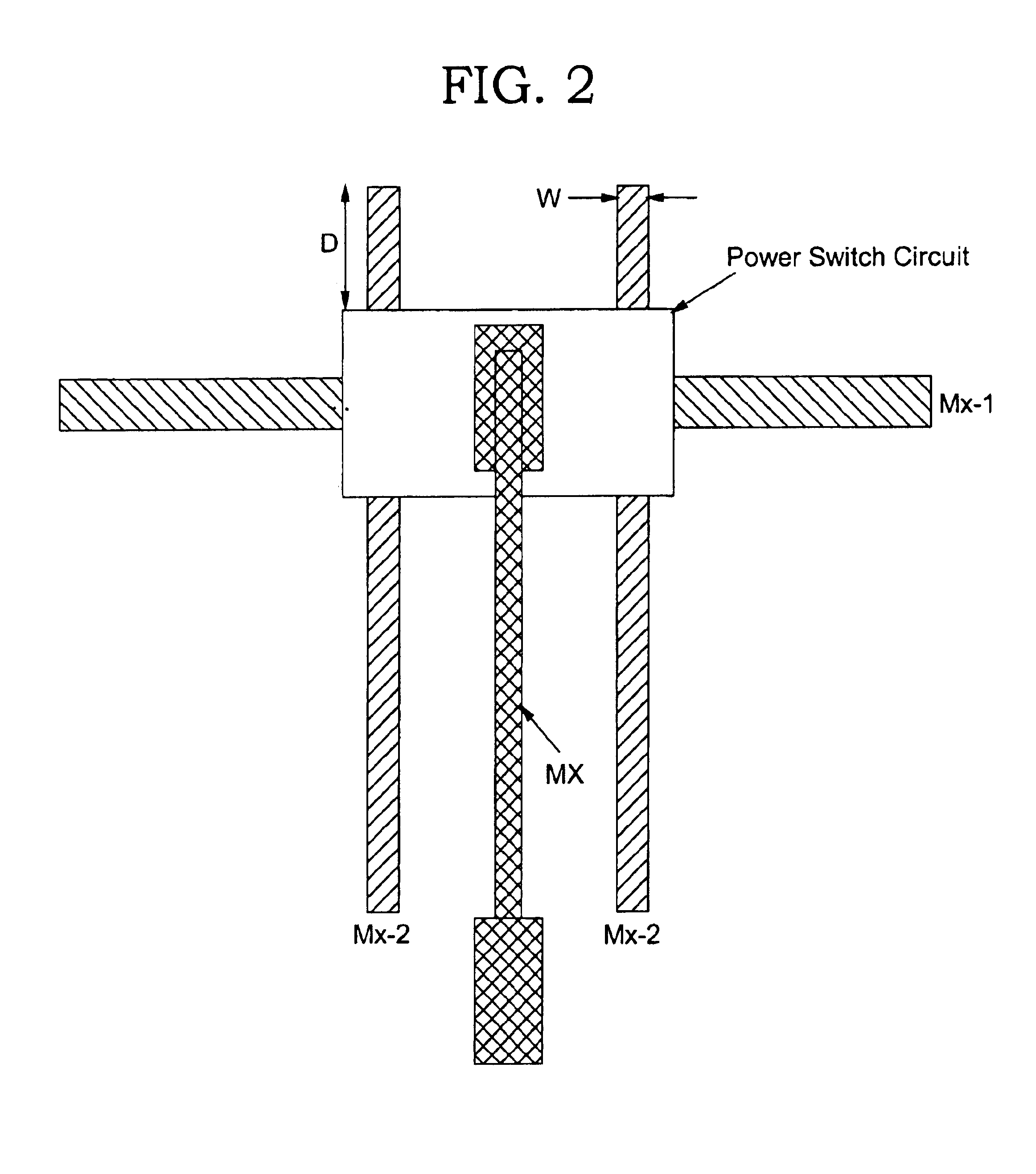
An integrated circuit structure has at least one voltage island and a pattern of power switches within the voltage island. The pattern determines the number of (and evenly spaces) the power switches according to the size of the serviceable area to which each of the power switches can provide power. The size of the power switches are matched to the current and voltage that will be provided by the power buses. The size of the serviceable area to which each of the power switches can provide power is dependent upon the size of the power switches.

Description

BACKGROUND OF THE INVENTION[0001]1. Field of the Invention[0002]The present invention generally relates to integrated circuits and more particularly to an improved integrated circuit design and method which utilizes voltage islands in application specific integrated circuit (ASIC) designs that make increasing use of power supply switching techniques to control chip power consumption.[0003]2. Description of the Related Art[0004]As technology scales for increased circuit density and performance, the need to reduce power consumption increases in significance as designers strive to utilize the advancing silicon capabilities. The consumer product market further drives the need to minimize chip power consumption.[0005]The total power consumed by conventional CMOS circuitry is composed of two primary sources. The first is active power consumed by circuits as they switch states and either charge or discharge the capacitance associated with the switching nodes. Active power represents the po...

Claims


Application Information

Patent Timeline
IPC IPC(8): H01L27/02H03K19/00H03K19/173H01LH01L27/00H01L27/118
CPCH01L27/0207H01L27/11898H01L27/00H01L27/02
Inventor BUFFET, PATRICK H.COHN, JOHN M.GROSSELFINGER, KEVIN M.LICHTENSTEIGER, SUSAN K.SMITH
Owner GLOBALFOUNDRIES US INC
Learn More