Area pattern processing of pixels

a processing field and area pattern technology, applied in static indicating devices, memory address/allocation/relocation, instruments, etc., can solve the problems of complex processing, large computational load on graphics systems, and high processing power of modern high-performance graphics systems

Inactive Publication Date: 2005-08-02
ORACLE INT CORP
View PDF2 Cites 33 Cited by
  • Summary
  • Abstract
  • Description
  • Claims
  • Application Information

AI Technical Summary

Benefits of technology

[0010]This area patterning circuit may advantageously allow the patterning of blocks having arbitrary origins with respect to the array pattern array.

Problems solved by technology

These new applications place tremendous computational loads upon graphics systems.
Consequently, modern high performance graphics systems incorporate graphics processors with a great deal of complexity and power, and the color value of one pixel may be the accumulated result of many calculations involving several models and mathematical approximations.
With each new generation of graphics system, there is more image data to process, the processing is more complex, and there is less time in which to process it.

Method used


Image

  • Area pattern processing of pixels
  • Area pattern processing of pixels
  • Area pattern processing of pixels

Examples


Embodiment Construction

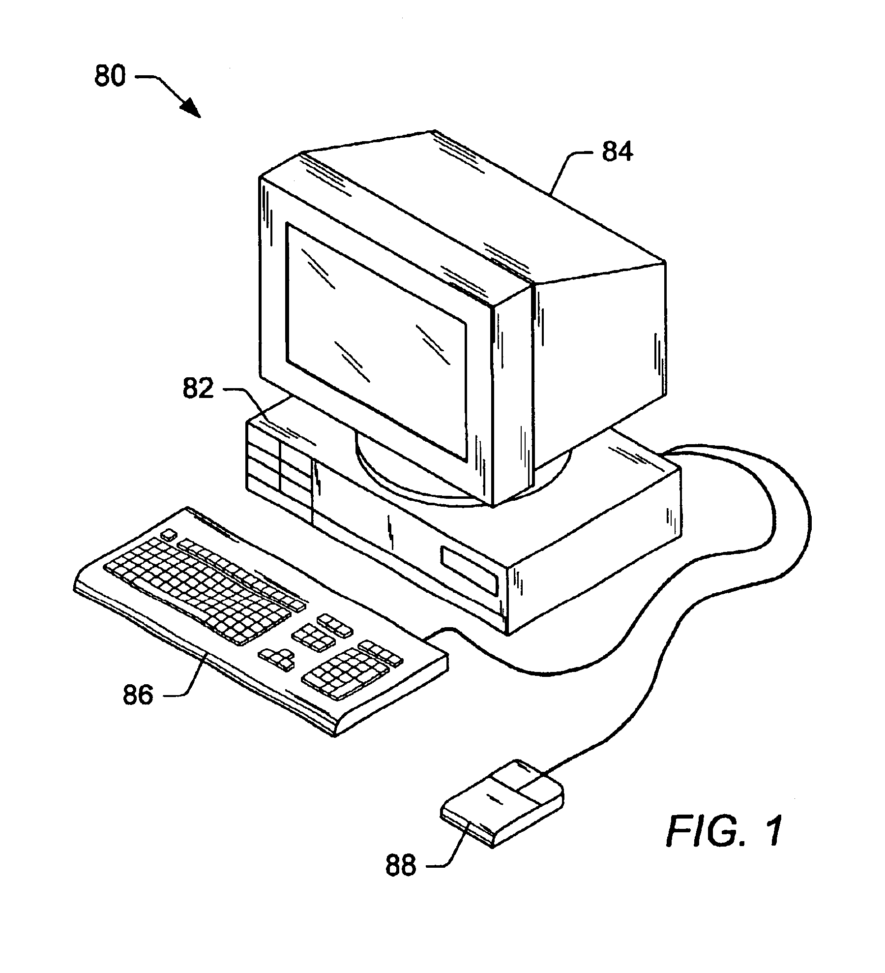
Computer System—FIG. 1

[0041]FIG. 1 illustrates one embodiment of a computer system 80 that includes a graphics system. The graphics system may be included in any of various systems such as computer systems, network PCs, Internet appliances, televisions (e.g. HDTV systems and interactive television systems), personal digital assistants (PDAs), virtual reality systems, and other devices which display 2D and / or 3D graphics, among others.

[0042]As shown, the computer system 80 includes a system unit 82 and a video monitor or display device 84 coupled to the system unit 82. The display device 84 may be any of various types of display monitors or devices (e.g., a CRT, LCD, or gas-plasma display). Various input devices may be connected to the computer system, including a keyboard 86 and / or a mouse 88, or other input device (e.g., a trackball, digitizer, tablet, six-degree of freedom input device, head tracker, eye tracker, data glove, or body sensors). Application software may be executed b...


PUM


Abstract

A circuit for outputting area pattern bits from an area pattern array. The circuit includes a first stage, second stage and third stage. The first stage is configured to output N adjacent scan lines from a 2N×2N area pattern array based on a first address. N is a positive integer. The second stage is configured to receive the N adjacent scanlines and to select an N×N block from the N adjacent scanlines based on a second address. The third stage is configured to (a) select an (N/2)×N region of bits from the N×N block and load bits of the (N/2)×N region into a set of pixel tag outputs in a first mode, and (b) select an N×(N/2) region of bits from the N×N block and load bits of the N×(N/2) region into the set of pixel tag outputs in a second mode.

Description

PRIORITY CLAIM[0001]This application claims priority to U.S. Provisional Application No. 60 / 363,654 filed on Mar. 12, 2002 entitled “Area Pattern Processing of Pixels in Super Sample Mode” invented by Steve M. Kurihara and Charles F. Patton. This Provisional Application is hereby incorporated by reference in its entirety as though fully and completely set forth herein.BACKGROUND OF THE INVENTION[0002]1. Field of the Invention[0003]This invention relates generally to the field of computer graphics and, more particularly, to a pipelined system and method for generating an area pattern for controlling various pixel operations within a graphics accelerator system.[0004]2. Description of the Related Art[0005]Early graphics systems were limited to two-dimensional (2D) graphics, were configured to compute a gray scale value for each pixel displayed, and acted as simple translators or interfaces to a display device. Modern high performance graphics systems, however, may support three-dimens...

Claims


Application Information

Patent Timeline
Patent Type & Authority Patents(United States)
IPC IPC(8): G09G5/395G06T15/00G09G5/393G09G5/36G09G5/14G09G5/06G09G5/08
CPCG06T15/005G09G5/363G09G5/393G09G5/395G09G5/06G09G5/08G09G5/14
Inventor KURIHARA, STEVEN M.PATTON, CHARLES F.
Owner ORACLE INT CORP
Why Eureka
Try Eureka