

Substrate processing apparatus and substrate processing method
a substrate processing and substrate technology, applied in the direction of photomechanical equipment, instruments, printers, etc., can solve the problem of difficulty in appropriately causing the microphase separation
- Summary
- Abstract
- Description
- Claims
- Application Information
AI Technical Summary
Benefits of technology
Problems solved by technology
Method used
Image

Examples
Embodiment Construction
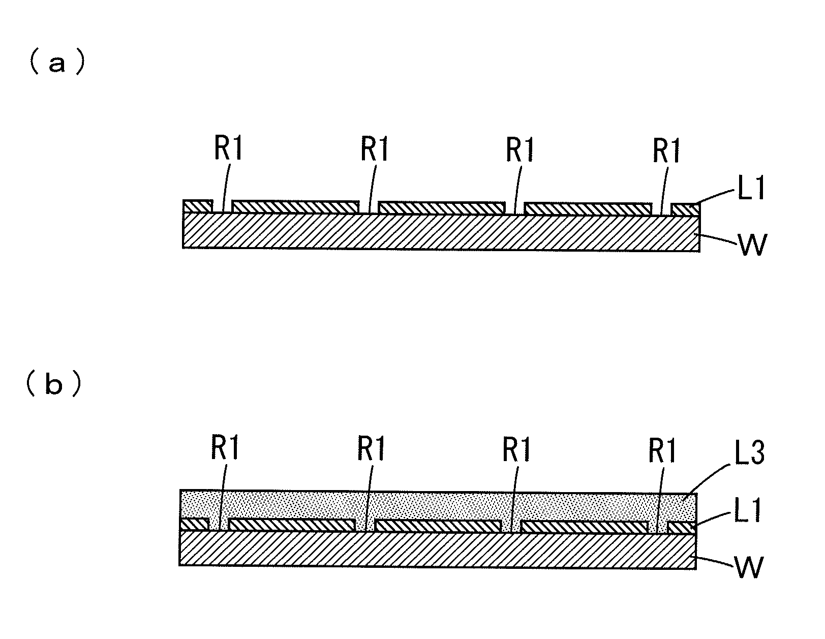
[0046]A substrate processing apparatus, a substrate processing method according to embodiments of the present invention will be described below with reference to the drawings. In the following description, a substrate refers to a semiconductor substrate, a substrate for a liquid crystal display, a substrate for a plasma display, a glass substrate for a photomask, a substrate for an optical disc, a substrate for a magnetic disc, a substrate for a magneto-optical disc, a substrate for a photomask or the like.
(1) Configuration of the Substrate Processing Apparatus
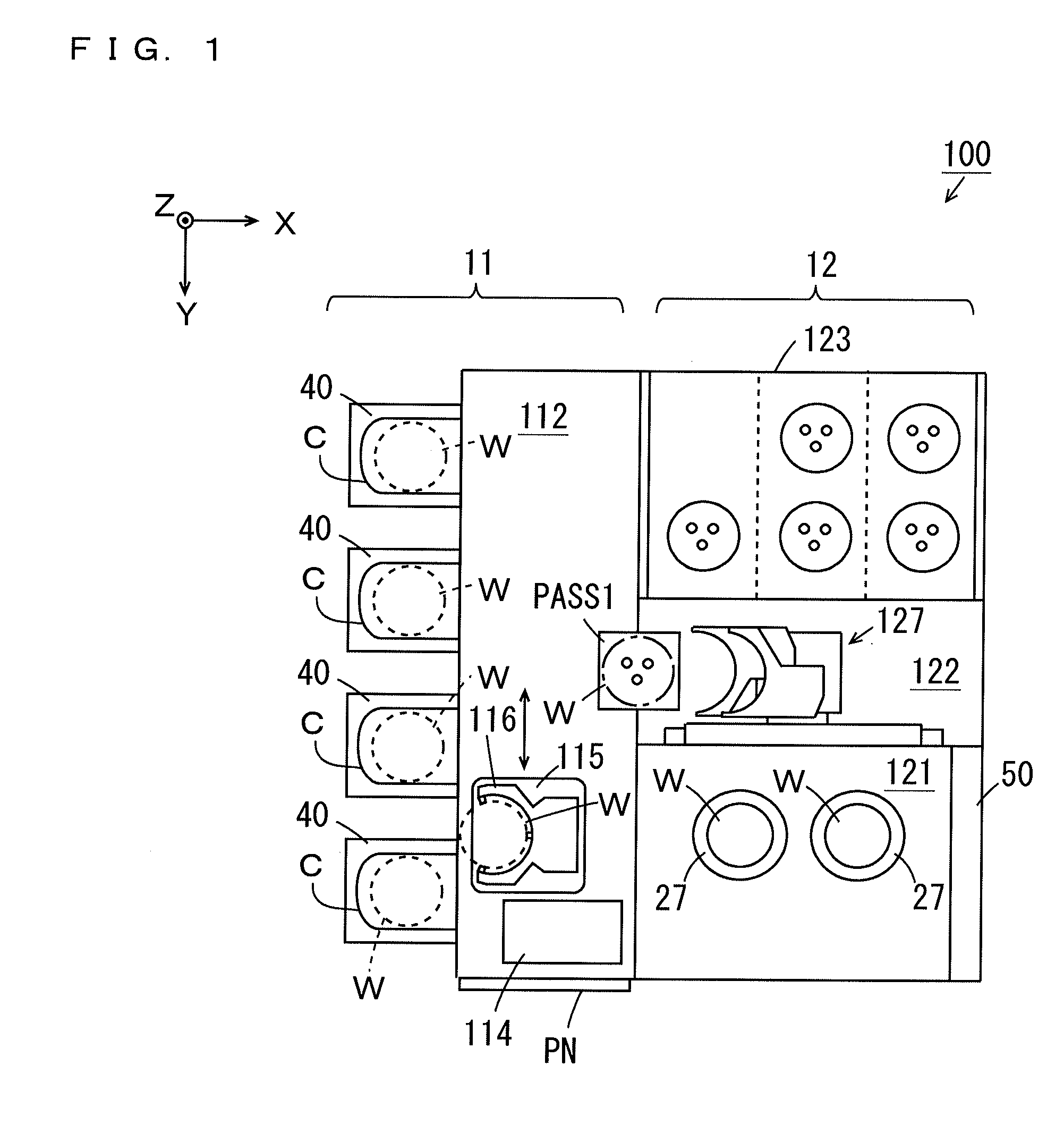
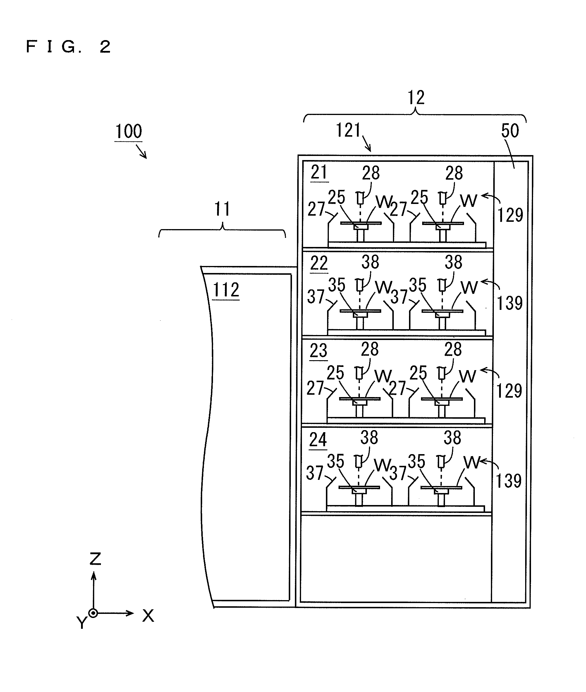
[0047]FIG. 1 is a schematic plan view of the substrate processing apparatus according to an embodiment of the present invention. FIGS. 1, 2 and subsequent given drawings are accompanied by the arrows that indicate X, Y, and Z directions orthogonal to one another for the clarity of a positional relationship. The X and Y directions are orthogonal to each other within a horizontal plane, and the Z direction corresponds to a verti...
PUM
| Property | Measurement | Unit |
|---|---|---|
| Temperature | aaaaa | aaaaa |
| Pressure | aaaaa | aaaaa |
Abstract
Description
Claims
Application Information