Light emitting device and manufacturing method thereof and display used this light emitting device

a technology of light emitting device and manufacturing method, which is applied in the direction of discharge tube luminescent screen, identification means, instruments, etc., can solve the problem of fatal deterioration of the (total) luminescent efficiency, the possibility of light emission is necessitated to have an upper limit, and the difficulty of forming the lens for light convergence or the reflection mirror on the side of the devi

Inactive Publication Date: 2005-02-03
SAMSUNG DISPLAY CO LTD
View PDF8 Cites 27 Cited by
  • Summary
  • Abstract
  • Description
  • Claims
  • Application Information

AI Technical Summary

Problems solved by technology

Further, organic EL devices involve certain limitations on the probability of the creation of singlet excited states of light-emitting material molecules on carrier recombination since the carrier recombination is dependent on spin statistics, thereby the probability of light emission is necessitated to have an upper limit.
In organic EL devices, having tight limitations on the light emission probability, low light extraction efficiency (low efficiency in extracting light from the organic EL device to outside) causes fatal deterioration of the (total) luminescent efficiency.
However, at a device whose pixel area is small, such as a dot matrix display, it is difficult to form the lenses for light convergence or form the reflection mirror on the side of the device.
Further, at the organic EL device, the thickness of the luminescent layer is less than a few μm, therefore, it is difficult to form the reflection mirror at the side of the device by tapering the side at the current fine processing technology.
If it is realized, the cost is increased largely.
This method has an effect to improve the light extracting efficiency to the forward, but cannot prevent the total internal reflection.
Therefore, while being effective for inorganic EL devices (including materials with large refractive indices), the method can not effectively improve the light extraction efficiency of organic EL devices (including light-emitting materials of relatively low refractive indices).
In these applications, it is necessary that each pixel for the RGB is formed separately, therefore, the forming process is very complicated, and it is disadvantageous to its mass production.
However, several times of the photo lithography process are required for forming the color filters or the light conversion layer and the process becomes quite complex.
Further, the surface of them becomes uneven.
Consequently, the performance of the organic EL device is decreased and the manufacturing cost is increased, that is, there are many problems at its mass production.
However, in this method, light emitted by an organic EL device (corresponding to a pixel area) tends to reach adjacent pixel areas, thereby the light leakage problem (light emission from pixel areas that are not supposed to emit light) occurs.
However, the method further deteriorates the light extraction efficiency, since part of the light emitted by the organic EL devices is absorbed by the black mask.
As described above, the prevention of light leakage and the improvement of light extraction efficiency in light-emitting devices employing organic EL devices are both still insufficient.

Method used


Image

  • Light emitting device and manufacturing method thereof and display used this light emitting device
  • Light emitting device and manufacturing method thereof and display used this light emitting device
  • Light emitting device and manufacturing method thereof and display used this light emitting device

Examples


Embodiment Construction

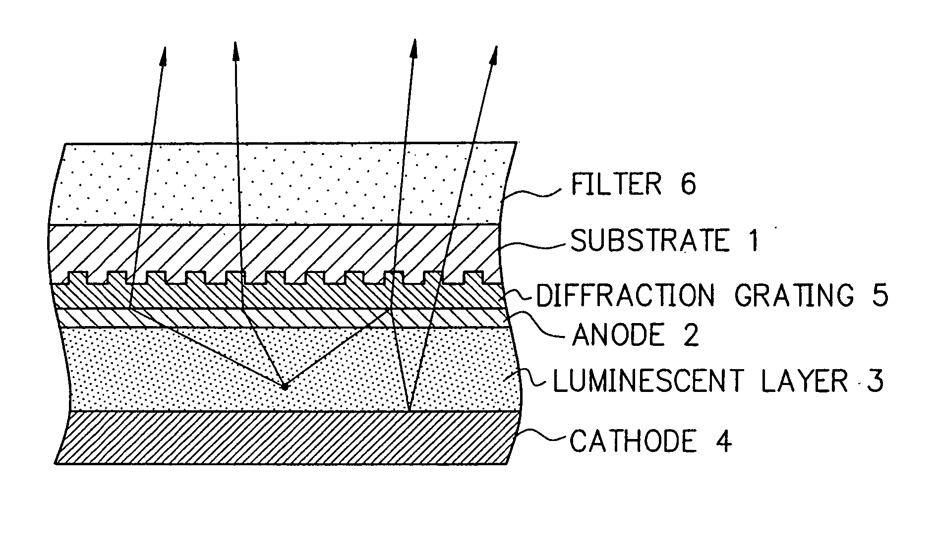
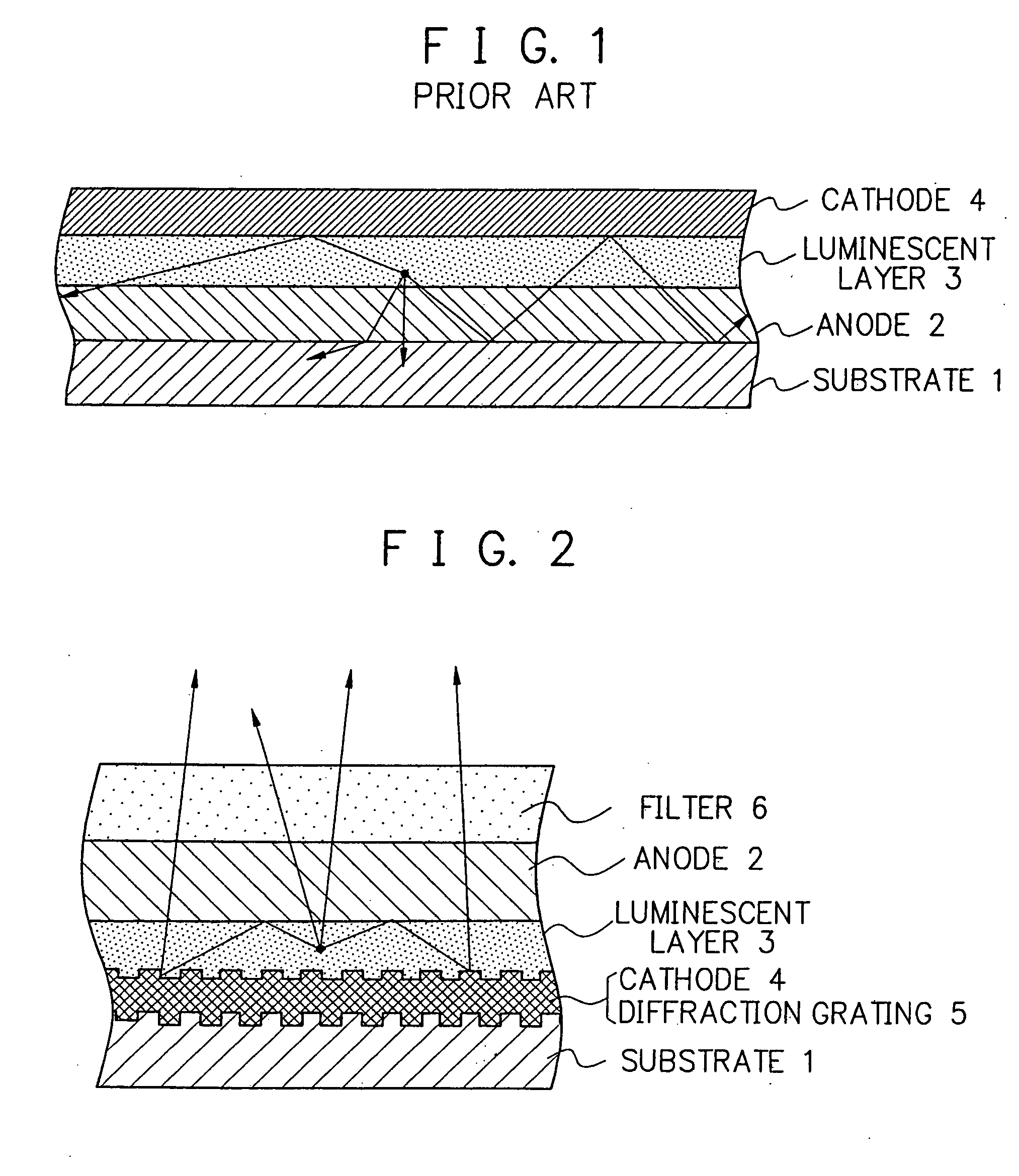
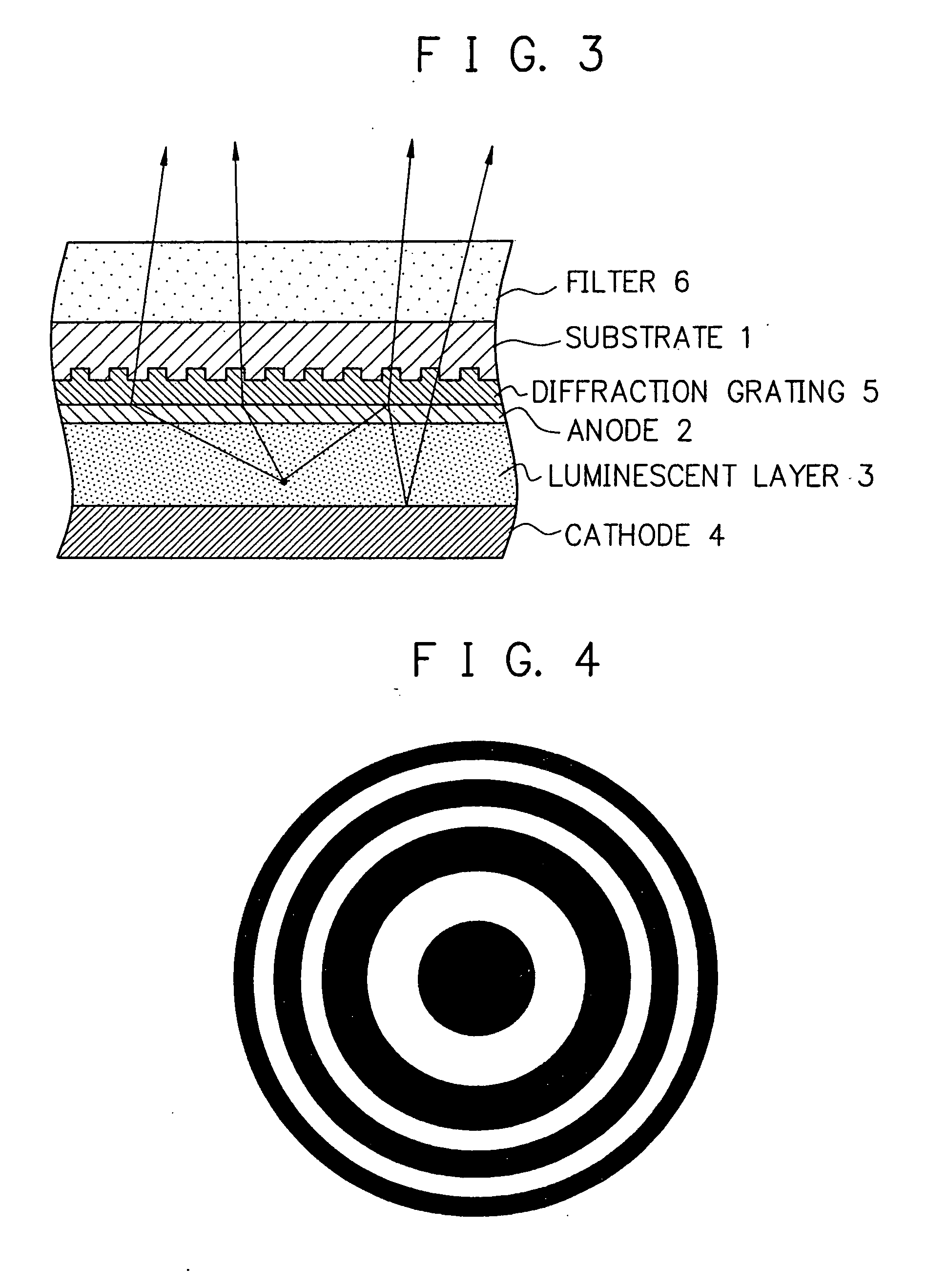
Referring now to the drawings, embodiments of the present invention are explained in detail. Japanese Patent No. 2991183 discloses an organic EL device. In this patent, it teaches that the light extracting efficiency is increased by combining an organic EL element with a diffraction grating or a zone plate. At the embodiments of the present invention, the emitting angle of light being extracted from an organic EL device is limited within a few degrees, by using a diffraction grating having a suitable grating pitch for light emitted from the organic EL device. With this, the light extracting efficiency is increased.

At the embodiments of the present invention, when a function is almost equal to that at the conventional technology, the same reference number is used.

As the diffraction grating at the embodiments of the present invention, both a reflection type and a transmission type can be used. FIG. 2 is a sectional view of a light emitting device using a reflection type diffracti...


PUM


Abstract

A light emitting device and a manufacturing method thereof and a display used the light emitting device, in which fine patterning for the light emitting device is realized by a simple process and the light leakage is prevented and the efficiency at extracting light is increased, are provided. The light emitting device provides an organic electroluminescent (EL) device in which electrodes and a luminescent layer are formed, a diffraction grating or a zone plate, and a filter. Light emitted from the luminescent layer transmits through the diffraction grating or the zone plate, which is formed with a designated grating pitch, or is reflected at the diffraction grating or the zone plate. With this, the transmitting or reflecting light is controlled to be in a designated angle region. And when the light is transmitted through the filter, light having different color tone and chromaticity from those of the light emitted from the luminescent layer is extracted.

Description

BACKGROUND OF THE INVENTION The present invention relates to a light emitting device and a manufacturing method thereof and a display used this light emitting device, in particular, which is an organic electroluminescent (EL) device that emits light having wide range wavelengths from blue to red. 1. Description of the Related Art An organic EL device is a self light emitting device, which makes use of the principle that when an electric field is applied, a fluorescent material emits light in response to the charge recombination of holes injected from an anode and electrons injected from a cathode. Since a report on a low-voltage-driven organic EL device employing multilayered structure was released by C. W. Tang et al. of Eastman Kodak Co. (C. W. Tang, S. A. VanSlyke, Applied Physics Letters, Vol. 51, page 913 (1987)), extensive researches have been made on organic EL devices, that is, EL devices employing organic materials. In the above report, an organic EL device employing t...

Claims


Application Information

Patent Timeline
Patent Type & Authority Applications(United States)
IPC IPC(8): G09F9/00G09F9/30H05B33/02H01L27/32H01L51/50H01L51/52H05B33/12H05B33/22H05B33/24H05B33/26
CPCH01L27/322H01L51/5237H01L51/5225H01L51/5275H01L2251/5315H01L51/5268H10K59/38H10K50/822H10K50/854H10K50/858H10K2102/3026H10K50/844H05B33/22
Inventor TOGUCHI, SATORUISHIKAWA, HITOSHIODA, ATSUSHI
Owner SAMSUNG DISPLAY CO LTD
Why Eureka
Try Eureka