Ultra-thin copper foil with carrier and printed wiring board using ultra-thin copper foil with carrier

a technology of copper foil and printed wiring board, which is applied in the direction of soldering apparatus, instruments, heat measurement, etc., can solve the problems of small peel strength between copper foil and substrate, difficult to produce printed wiring board with reliable and fine wiring pattern, and failure of insulation, so as to improve peel strength and easy etching

Inactive Publication Date: 2005-07-21
FURUKAWA ELECTRIC CO LTD
View PDF9 Cites 26 Cited by
  • Summary
  • Abstract
  • Description
  • Claims
  • Application Information

AI Technical Summary

Benefits of technology

[0067] In the above case, that is using sulfuric acid solution or sulfuric acid-copper sulfamate solution, excepting for using alternate current or PR current (± inverted direct current), small pit is occurred on the surface of the ultra-thin copper foil and peel strength with the resin substrate is improved. Further, since also in this case the roughening grains leading to “treatment transfer after etching”, when etching wiring, fine wiring can be formed.
[0068] In the case of using sulfuric acid solution or sulfuric acid-copper sulfamate solution and the case that using alternate current and PR current (± inverted direct current), small copper nodule is deposited with occurring pit. However, in this case, since small copper nodule is a thing that a portion of the ultra-thin copper foil is re-deposited and composition of it is equal to the ultra-thin copper foil in itself, in comparison with a conventional roughening treatment grain, when pattern is etched, small copper nodule is easily etched and “treatment transfer after etching” is hardly occurred. Therefore, finer pattern can be formed.
[0069] In the copper foil of the present invention, since the roughening grain of which etching speed is slower than the copper foil in itself is not deposited on the surface of the copper foil, when wiring is etched, “treatment transfer after etching” is not occurred, and fine wiring of 15 μm or less can be formed. Even after etching lines of 15 μm or less, since chemical treatment and / or electrochemical treatment that improve peel strength with the resin are performed, the microscopic lines and the wiring substrate (resin substrate) have large peel strength.

Problems solved by technology

These problems are not serious in the case that the line width of wiring in the formed wiring pattern, however, it may lead to disconnection in the case of the wiring pattern of which line width is narrow.
Consequently, until the embedded protrusion of the copper grains is removed completely from the substrate, a copper remains (this phenomenon is usually called as treatment transfer after etching, it may be a cause that insulation failure is occurred in the case that the pitches of adjacent lines of the wiring pattern is narrow.
In the case of using a thin copper foil, in fact, such a problem can be solved if the surface roughness is made smaller, however, in that case, it is difficult to produce the printed wiring board having the reliable and fine wiring pattern, since the peel strength between the copper foil and the substrate becomes smaller.
Moreover, in the case of the thin copper foil, since the mechanical strength is small, wrinkles and creases cause easily, further the copper foil may go out when producing a printed wiring board, therefore there is a problem that the greatest care is required for handling.
As mentioned above, it is considerably difficult to produce a printed wiring board having fine wiring pattern that the Ef value is large and that the peel strength is large as a practical matter.

Method used


Image

  • Ultra-thin copper foil with carrier and printed wiring board using ultra-thin copper foil with carrier
  • Ultra-thin copper foil with carrier and printed wiring board using ultra-thin copper foil with carrier
  • Ultra-thin copper foil with carrier and printed wiring board using ultra-thin copper foil with carrier

Examples


first embodiment

The First Embodiment

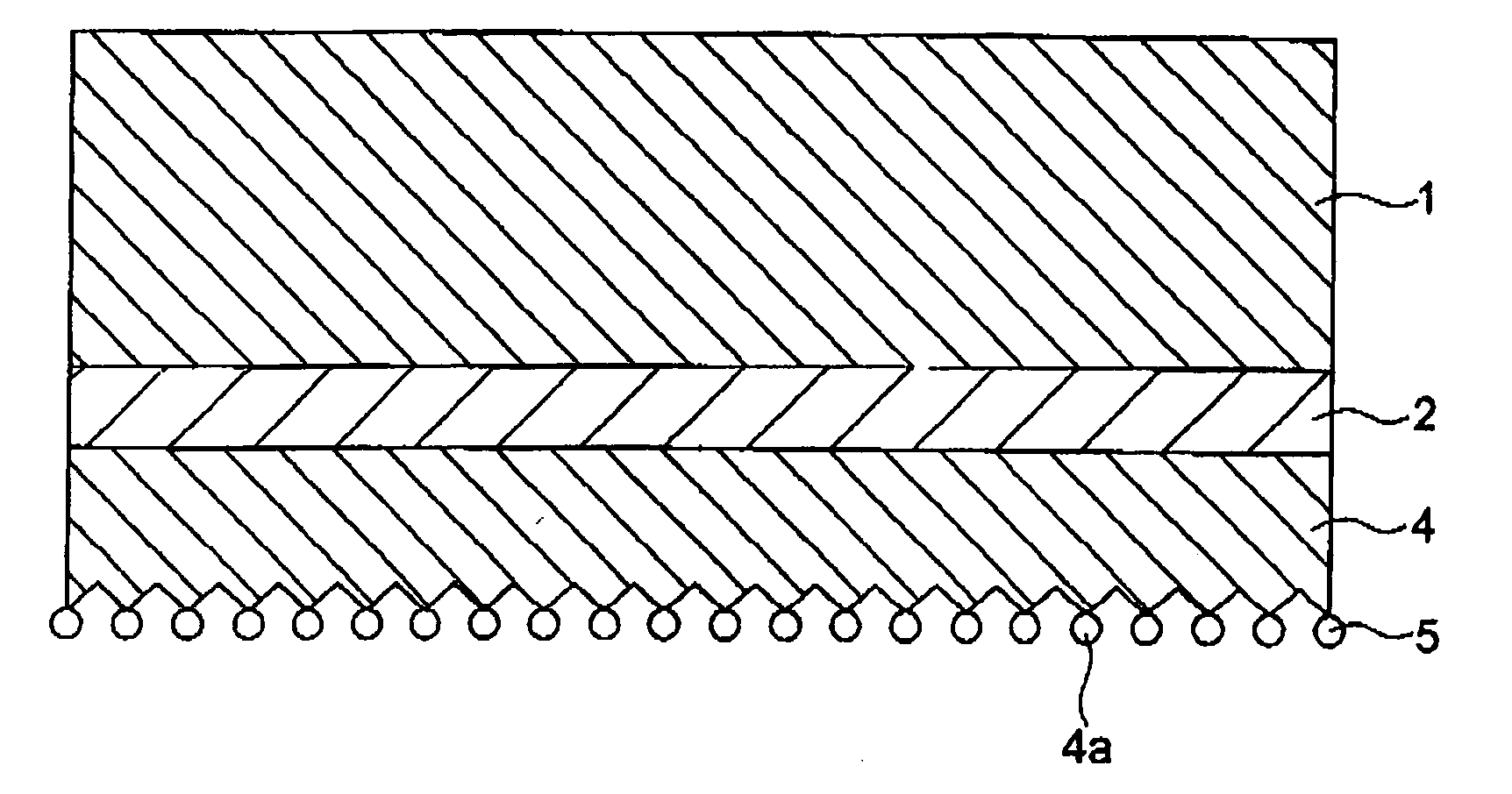
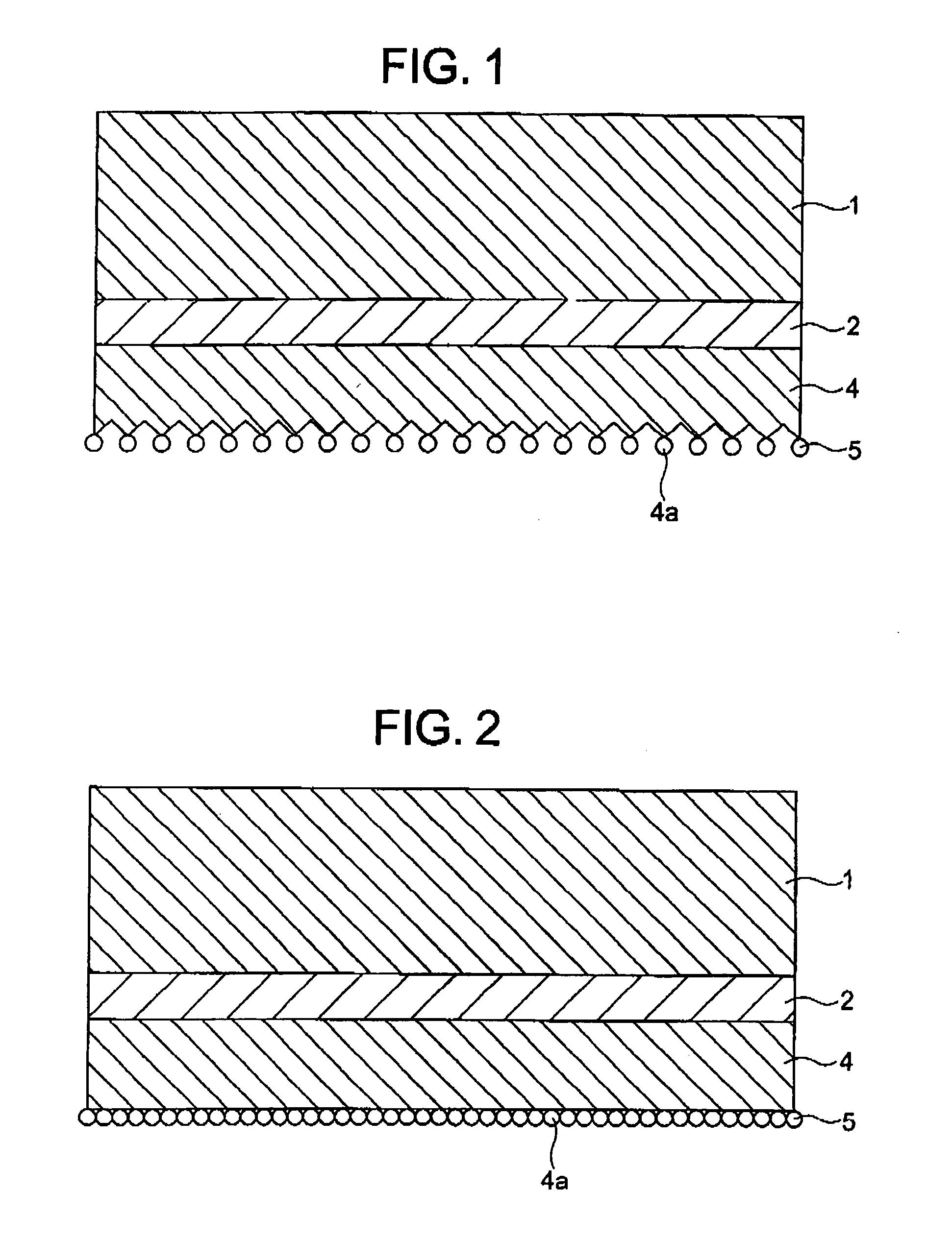
[0085]FIG. 2 shows an ultra-thin copper foil with a carrier foil of the first embodiment of the present invention, a peeling layer 2 is formed on the surface of a carrier foil 1, and an ultra-thin copper foil 4 is formed on the peeling layer 2. The ultra-thin copper foil with a carrier foil of the first embodiment of the present invention is constituted by laminating the carrier foil 1, the peeling layer 2 and the ultra-thin copper foil 4.

[0086] The surface roughness Rz of the surface of the ultra-thin copper foil 4 is 2.5 μm or less and the minimum distance between peaks of salients of a based material is 5 μm or more, and a roughening grain layer 5 consisting of roughening grains 4a is formed on the surface.

[0087] To produce the surface of the ultra-thin copper foil 4 of which the surface roughness Rz is 2.5 μm or less and the minimum distance between peaks of salients of a based material is 5 μm or more, plating is formed by a copper plating solution that ca...

example 1

[0099] (1) Making of an Ultra-Thin Copper Foil

[0100] An untreated electrolytic copper foil having the surface (S surface) roughness of 1.2 μm and the thickness of 35 μm was defined as a carrier foil and on the S surface chromium electroplating was successively performed, a chromium plating layer (peeling layer) of the thickness of 0.005 μm was formed. Next, by using a copper sulfate solution described in the following composition 1 as an electrolytic solution and performing the electrolysis in a condition that the current density was 30 A / dm2 and the temperature of the solution was 50 degrees C., an ultra-thin copper layer (copper foil) having the thickness of 5 μm was electroplated.

(Composition 1)copper sulfate (CuSO4.5H2O) 250 g / l to 350 g / lsulfuric acid (H2SO4)  80 g / l to 120 g / l3-mercapto-1-sodium propanesulfonate 0.5 ppm to 5 ppmhydroxyethyl cellulose  1 ppm to 10 ppmlow-molecular-weight glue (molecular weight 3000)  1 ppm to 10 ppmCl−  10 ppm to 50 ppm

[0101] On the ultra-th...

example 2

[0103] (1) Producing an Ultra-Thin Copper Layer

[0104] An untreated electrolytic copper foil having the surface (S surface) roughness of 1.2 μm and the thickness of 35 μm was defined as a carrier foil and on the S surface chromium electroplating was successively performed, a chromium plating layer (peeling layer) of the thickness of 0.005 μm was formed. Next, by using a copper sulfate solution described in the following composition 1 as an electrolytic solution and performing the electrolysis in a condition that the current density was 10 A / dm2 and the temperature of the solution was 35 degrees C., an ultra-thin copper layer (copper foil) having the thickness of 5 μm was electroplated.

(Composition 2)copper sulfate (CuSO4.5H2O) 240 g / lsulfuric acid (H2SO4)  60 g / lcupracid 210 by Nihon Schering K.K.make up agent 0.5 cc / lbrightening agent (A) 0.5 cc / lbrightening agent (B)using for only complementCl−  30 ppm

Note that as the complement of the brightening agent, the brightening agent (A...


PUM

PropertyMeasurementUnit
surface roughnessaaaaaaaaaa
grains diameteraaaaaaaaaa

Abstract

To produce an ultra-thin copper foil with a carrier foil that microscopic crystal grains can be deposited without being affected by the surface roughness of a carrier foil, etching can be performed until an ultra-fine width such that line/space is 15 μm or less, and the microscopic line and a wiring board have large peel strength even after line of 15 μm is etched. An ultra-thin copper foil wherein a carrier foil, a peeling layer, an ultra-thin copper foil are laminated in this order, the ultra-thin copper foil (before roughening treatment is performed) is an electrolytic copper foil that surface roughness of 2.5 μm as ten point height of roughness profile, and the minimum distance between peaks of salients of a based material is 5 μm or more. Moreover, the surface of the ultra-thin copper foil is performed roughening treatment.

Description

BACKGROUND OF THE INVENTION [0001] 1. Field of the Invention [0002] The present invention relates to an ultra-thin copper foil with a carrier foil used at the time of producing a printed wiring board. In particular, the present invention relates to an ultra-thin copper foil with a carrier foil used preferably for producing a printed wiring board for high density ultra-fine wiring or a multilayer printed wiring board. [0003] 2. Description of the Related Art [0004] A printed wiring board is produced as mentioned below. [0005] First, after placing a thin copper foil for forming a surface circuit on a surface of an insulative substrate consisting of a glass epoxy resin or a polyimide resin and so on, by heating and laminating, a copper clad laminate is produced. [0006] Next, after placing a through hole and a through hole plating are performed sequentially, an etching process is performed to a copper foil in the surface of the copper clad laminate, a wiring pattern having a desired lin...

Claims


Application Information

Patent Timeline
Patent Type & Authority Applications(United States)
IPC IPC(8): H05K1/09C25D5/48C25D7/06H05K3/02H05K3/38
CPCC25D5/48Y10T428/12438H05K3/025H05K3/383H05K3/384Y10T428/12493Y10T428/265Y10T428/12472Y10T428/12514Y10T428/12903Y10T428/24802Y10T428/12028Y10T428/12993Y10T428/24917Y10T428/12569C25D7/0614C25D1/04H05K1/09H05K3/38
Inventor SUZUKI, AKITOSHIFUKUDA, SHIN
Owner FURUKAWA ELECTRIC CO LTD
Why Eureka
Try Eureka