Integrated circuit substrate having laser-embedded conductive patterns and method therefor

a technology of integrated circuit substrate and laser-embedded conductive pattern, which is applied in the direction of conductive pattern formation, semiconductor/solid-state device details, printed element electric connection formation, etc., can solve the problem of limiting the resolution of printed circuits to control interconnect density, cost limitations, and the level of interconnect density is less than desirabl

Inactive Publication Date: 2005-08-16
AMKOR TECH SINGAPORE HLDG PTE LTD
View PDF25 Cites 230 Cited by
  • Summary
  • Abstract
  • Description
  • Claims
  • Application Information

AI Technical Summary

Problems solved by technology

The resolution of the printed circuit is often the limiting factor controlling interconnect density.
Photo-etch and other processes for developing a printed circuit on a substrate have resolution limitations and associated cost limitations that set the level of interconnect density at a level that is less than desirable for interfacing to present integrated circuit dies that may have hundreds of external connections.
However, reducing inter-conductor spacing has a disadvantage that migration and shorting may occur more frequently for lowered inter-conductor spacings, thus setting another practical limit on the interconnect density.

Method used


Image

  • Integrated circuit substrate having laser-embedded conductive patterns and method therefor
  • Integrated circuit substrate having laser-embedded conductive patterns and method therefor
  • Integrated circuit substrate having laser-embedded conductive patterns and method therefor

Examples


Embodiment Construction

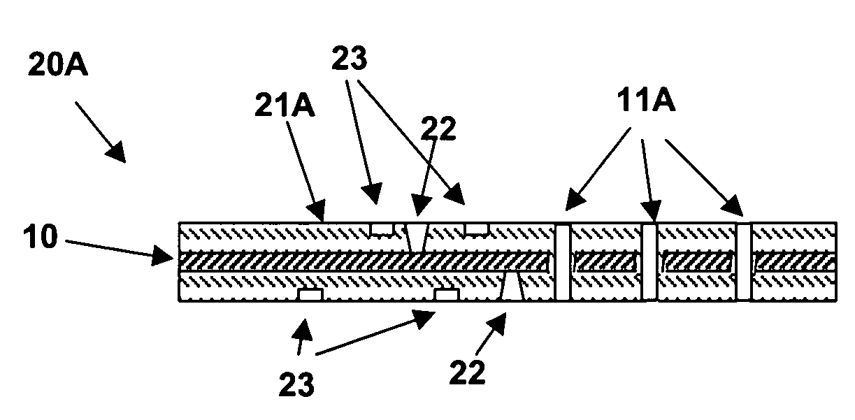
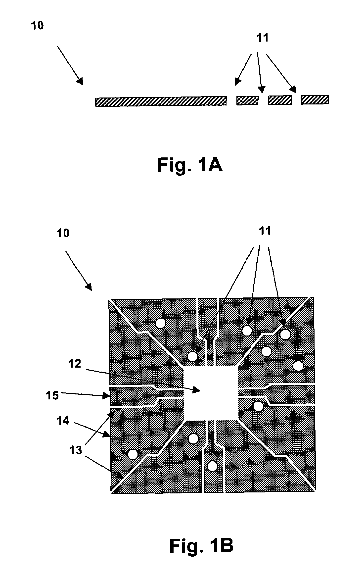
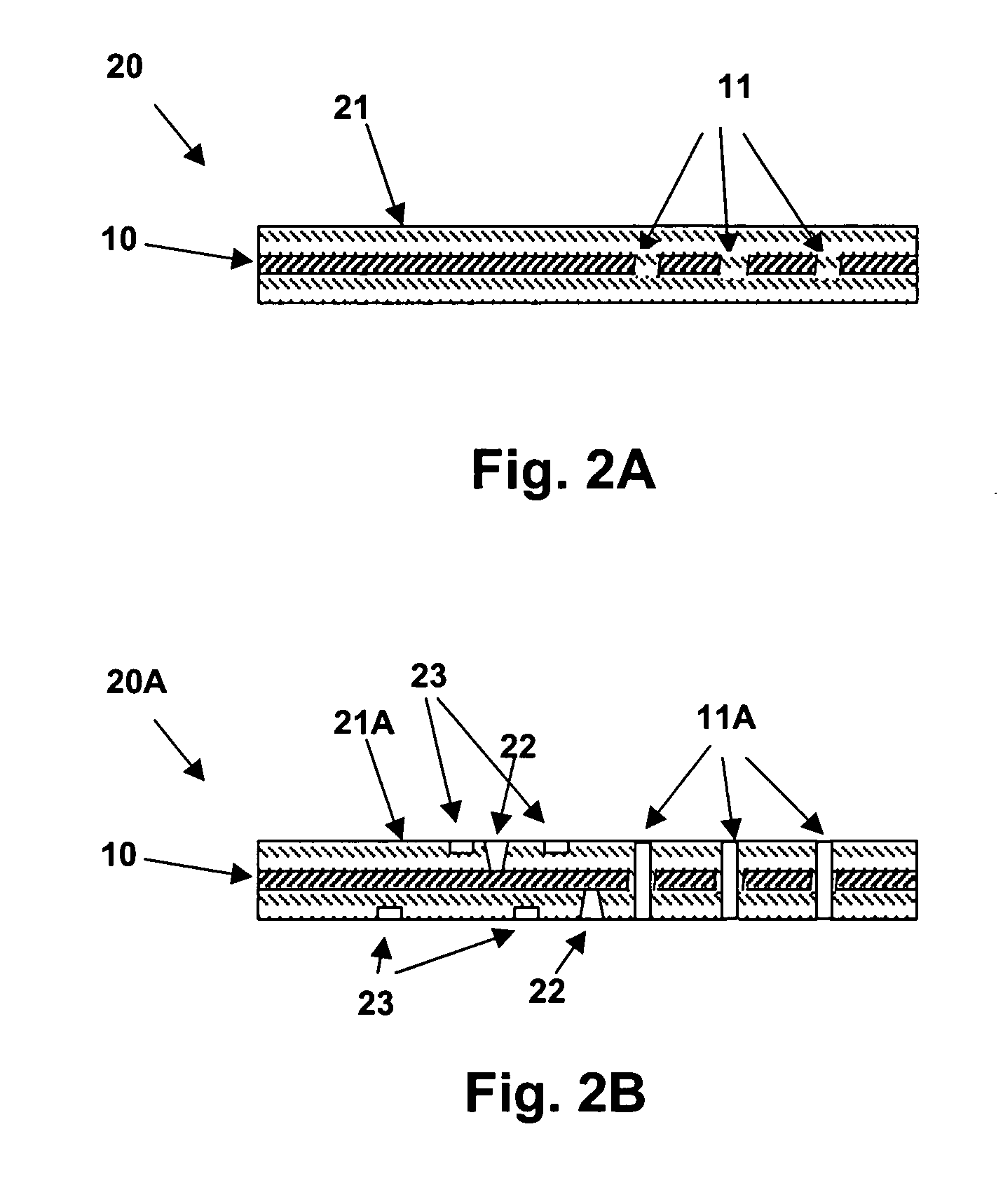
[0013]The above-incorporated patent application discloses a process and structure for manufacturing a low-cost substrate having high conductor density and electrical integrity by embedding the conductive patterns beneath the surface of a substrate. The substrate is an embossed substrate requiring tooling to form channels for the conductive patterns. While embossing provides a low cost and high throughput manufacturing process for the substrate base, the tooling must be remanufactured when design changes are made, as it is unique to a particular design. For low volume applications such as prototyping, the cost to tool the embossing process may be prohibitive and in general, the techniques of the present invention will provide a lower cost alternative, except in designs or portions of designs that have large areas that are recessed such as wells for integrated circuit dies.

[0014]The present invention provides an alternative that does not require custom tooling for producing channels f...


PUM

PropertyMeasurementUnit
electricallyaaaaaaaaaa
dielectricaaaaaaaaaa
conical shapeaaaaaaaaaa

Abstract

An integrated circuit substrate having laser-embedded conductive patterns provides a high-density mounting and interconnect structure for integrated circuits. Conductive patterns within channels on the substrate provide interconnects that are isolated by the channel sides. A dielectric material is injection-molded or laminated over a metal layer that is punched or etched. The metal layer can provide one or more power planes within the substrate. A laser is used to ablate channels on the surfaces of the outer dielectric layer for the conductive patterns. The conductive patterns are electroplated or paste screen-printed and an etchant-resistive material is applied. Finally, a plating material can be added to exposed surfaces of the conductive patterns. An integrated circuit die and external terminals can then be attached to the substrate, providing an integrated circuit having a high-density interconnect.

Description

CROSS-REFERENCE TO RELATED APPLICATIONS[0001]The present application is related to U.S. patent application Ser. No. 09 / 931,144 filed Aug. 16th, 2001 by the same inventors and assigned to the same assignee. The specification of the above-referenced patent is herein incorporated by reference.FIELD OF THE INVENTION[0002]The present invention relates generally to semiconductor packaging, and more specifically, to a substrate having laser-embedded conductive patterns for providing electrical inter-connection within an integrated circuit package.BACKGROUND OF THE INVENTION[0003]Semiconductors and other electronic and opto-electronic assemblies are fabricated in groups on a wafer. Known as “dies”, the individual devices are cut from the wafer and are then bonded to a carrier. The dies must be mechanically mounted and electrically connected to a circuit. For this purpose, many types of packaging have been developed, including “flip-chip”, ball grid array and leaded grid array among other mo...

Claims


Application Information

Patent Timeline
Patent Type & Authority Patents(United States)
IPC IPC(8): H01L21/48H01L21/02H05K7/10H05K3/00H05K3/42H05K1/05H05K3/10H05K3/12
CPCH01L21/4857H05K3/107H05K3/1258H05K7/1061H01L24/73Y10T29/49146H01L2224/16H01L2224/48091H01L2924/01029H01L2924/01078H01L2924/01079H01L2924/01082H01L2924/14H01L2924/15311H05K1/056H05K3/0032H05K3/0035H05K3/423H05K2201/09036H05K2201/09554H05K2203/0723Y10T29/49165Y10T29/4913Y10T29/49126Y10T29/49155Y10T29/49167H01L2924/1815H01L2224/48227H01L2224/73265H01L2224/32225H01L2924/014H01L2924/01005H01L2924/01006H01L2924/01033H01L2924/01047H01L2924/00014H01L2924/00012H01L2924/00H01L2924/15747
Inventor HUEMOELLER, RONALD PATRICKRUSLI, SUKIANTO
Owner AMKOR TECH SINGAPORE HLDG PTE LTD
Why Eureka
Try Eureka