Semiconductor device for reading signal from photodiode via transistors

a transistor and photodiode technology, applied in the direction of radio frequency controlled devices, instruments, television systems, etc., can solve the problems of junction leak current reduction, difficult wiring layout, and difficult light convergence of micro lenses, so as to reduce junction leak current and improve image quality

Active Publication Date: 2005-08-16
FUJITSU SEMICON LTD
View PDF4 Cites 41 Cited by
  • Summary
  • Abstract
  • Description
  • Claims
  • Application Information

AI Technical Summary

Benefits of technology

[0016]An object of this invention is to provide a semiconductor device capable of raising a ratio of an area occupied by a photodiode of a pixel.
[0017]Another object of the invention is to provide a semiconductor device capable of reducing junction leak current and improving an image quality.

Problems solved by technology

If the area of one pixel is made small in order to improve a pixel density, light convergence of a micro lens becomes difficult.
Since the upper level wiring lines cannot run in the region where the photodiode PD is disposed, the wiring layout is not easy.
A significant issue of a CMOS solid state imaging device is concerned about reduction in junction leak current.
A pixel having a large junction leak current becomes a white dot which degrades the image quality.
This contact of the plug is one factor of increasing junction leak current.

Method used


Image

  • Semiconductor device for reading signal from photodiode via transistors
  • Semiconductor device for reading signal from photodiode via transistors
  • Semiconductor device for reading signal from photodiode via transistors

Examples


first embodiment

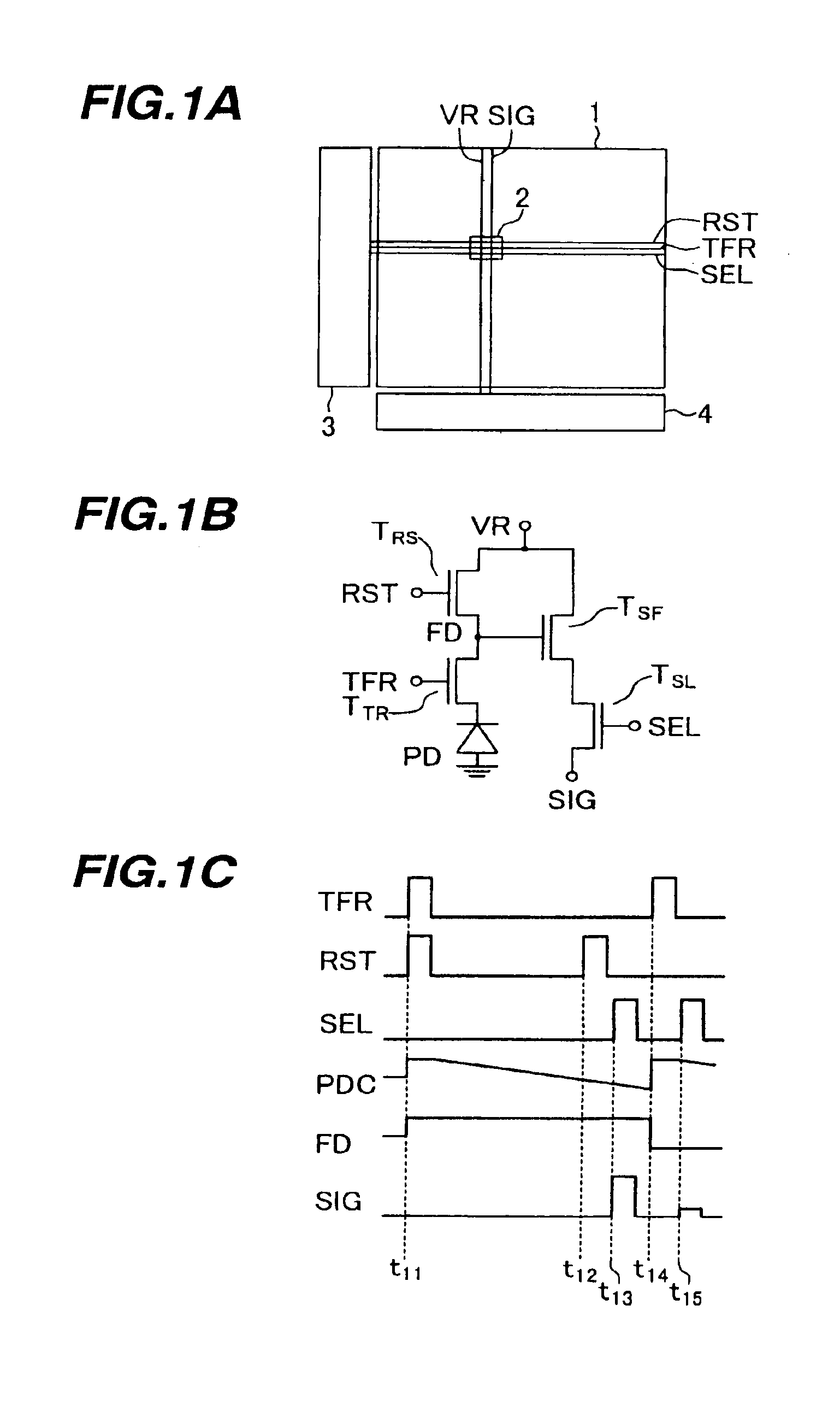
[0033]FIG. 1A is a block diagram of a four-transistor solid state imaging device (image sensor) according to the invention. A plurality of pixels 2 are disposed in an imaging area in a matrix shape. In correspondence with each of pixel rows, a reset signal line RST, a transfer signal line TFR and a select signal line SEL are disposed. In correspondence with each of pixel columns, a signal read line SIG and a reset voltage supply line VR are disposed.

[0034]A row select circuit 3 sends electric signals to the reset signal line RST, transfer signal line TFR and select signal line SEL at timings to be described later. An image signal is input from each pixel 2 to a read circuit 4 via the signal read line SIG.

[0035]FIG. 1B is an equivalent circuit diagram of one pixel. One pixel comprises a photodiode PD, a transfer transistor TTR, a reset transistor TRS, a source follower transistor TSF and a select transistor TSL. These transistors are all made of n-channel transistors.

[0036]The drain ...

second embodiment

[0086]Next, by referring to FIGS. 4A to 4D, a four-transistor solid state imaging device will be described.

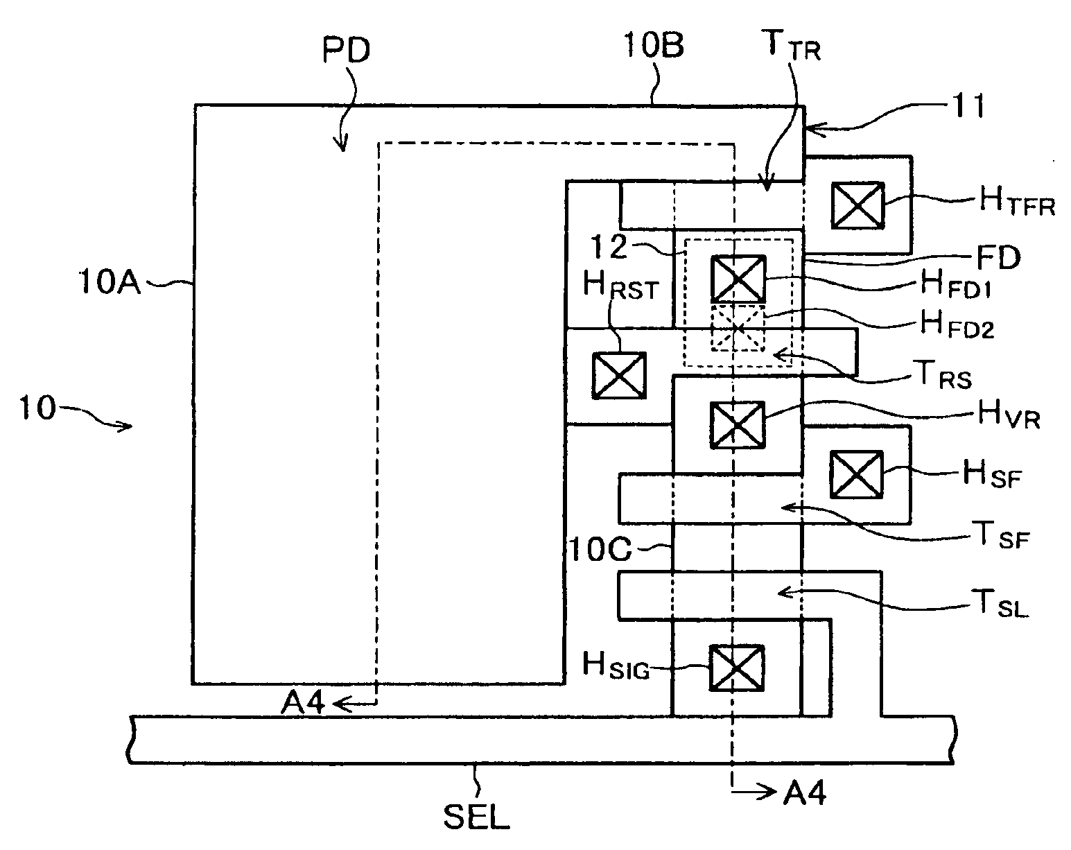
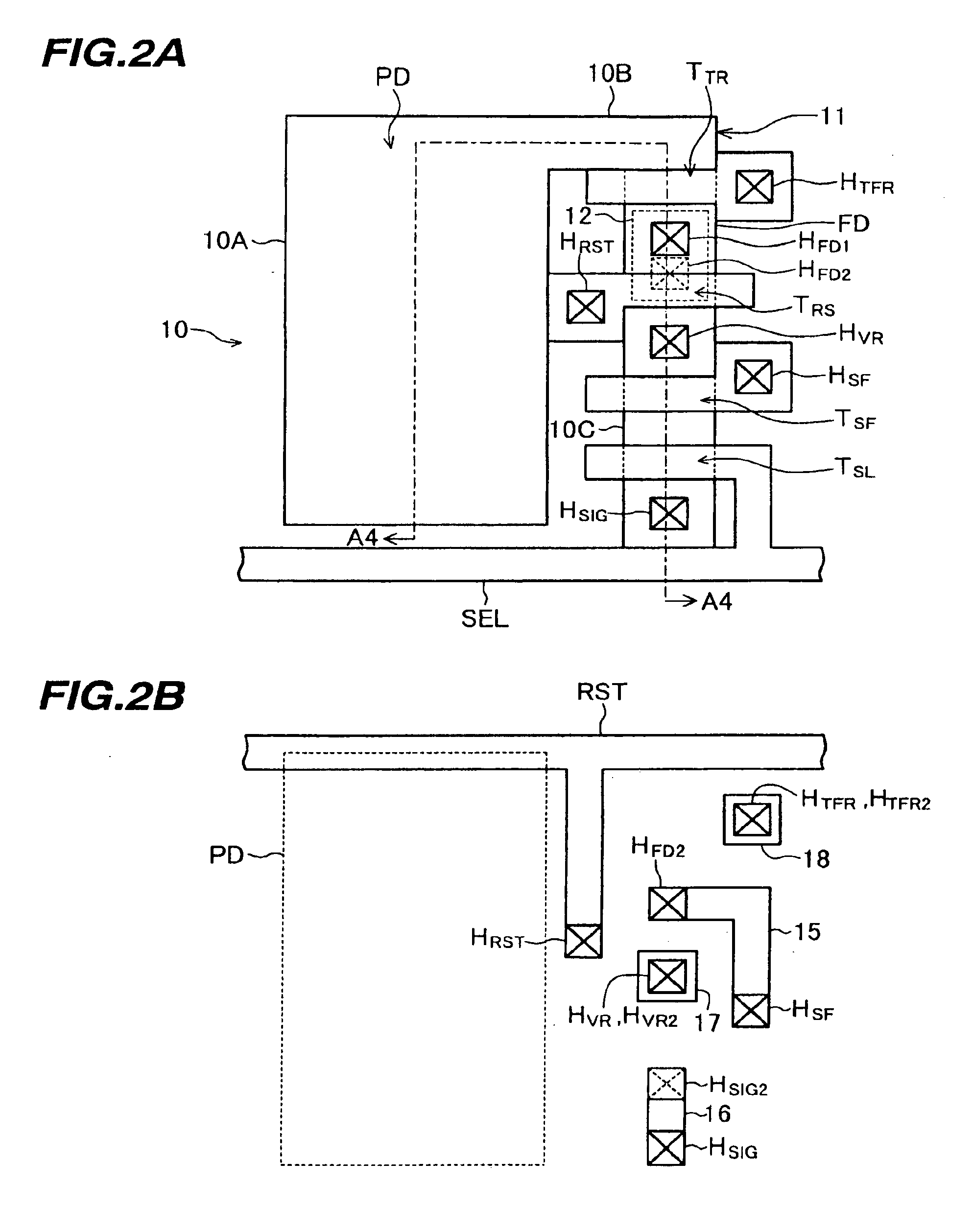
[0087]FIG. 4 is a plan view of one pixel of the four-transistor solid state imaging device of the second embodiment. The layout of an active region 10, each transistor, via holes, and a select signal line SEL is similar to the layout of these elements of the solid state imaging device of the first embodiment shown in FIG. 2A.

[0088]FIG. 4B shows the pattern of a silicon wiring layer corresponding to the silicon film 12 of the first embodiment shown in FIG. 2A. An intra-pixel wiring line 15A is connected to a floating diffusion region FD via a via hole HFD1, and to the gate electrode of a source follower transistor TSF via a via hole HSF. A reset signal line RST extending in the row direction is connected to the gate electrode of a reset transistor TRS via the via hole HRST.

[0089]The intra-pixel wiring line 15A and reset signal line RST have a two-layer structure of an amorphous...

third embodiment

[0094]Next, by referring to FIGS. 5A to 6E, a four-transistor solid state imaging device will be described.

[0095]FIG. 5A is a plan view of one pixel of the solid state imaging device of the third embodiment. Description will be given on different points from the structure of the solid state imaging device of the first embodiment shown in FIG. 2A.

[0096]In the first embodiment, the gate electrodes of the transistors and the via holes above the impurity diffusion region are disposed with some position alignment margin. In the third embodiment, as will be later described, via holes are formed in self alignment with gate electrodes. Therefore, the distance between the gates of a transfer transistor TTR, a reset transistor TRS, a source follower transistor TSF and a select transistor TSL is shorter than the distance between the gates of the first embodiment shown in FIG. 2A. Further, via holes HTFR, HRST and HSF for interconnecting gate electrodes and upper wiring layers are disposed wit...


PUM


Abstract

Pixels are disposed on a semiconductor substrate in a matrix shape. Each pixel includes a photodiode, a reset transistor, a source follower transistor and a select transistor. An active region in which the photodiode and transistors are disposed includes a first area in which the photodiode is disposed and a second area having an are elongated in a first direction. Each of the gate electrodes of the reset transistor, source follower transistor and select transistor crosses the area, elongated in the first direction, of the second area. An intra-pixel wiring line interconnects the drain region of the reset transistor and the gate electrode of the source follower transistor.

Description

CROSS REFERENCE TO RELATED APPLICATION[0001]This application is based on Japanese Patent Application No. 2002-251265 filed on Aug. 29, 2002, the entire contents of which are incorporated herein by reference.BACKGROUND OF THE INVENTION[0002]A) Field of the Invention[0003]The present invention relates to a semiconductor device for reading an electric signal of each of a plurality of pixels disposed on a semiconductor substrate to a signal read line via transistors, the electric signal being photoelectrically converted by a photodiode of the pixel.[0004]B) Description of the Related Art[0005]A solid state imaging device (image sensor) manufactured based upon complimentary MOS (CMOS) processes generally uses an active pixel sensor (APS) in whose pixel is constituted of: a photodiode for conducting photoelectric conversion; a reset transistor for initializing a voltage to be applied to the photodiode; a source follower transistor for converting signal charges of the photodiode into a vol...

Claims


Application Information

Patent Timeline
Patent Type & Authority Patents(United States)
IPC IPC(8): H01L27/146H04N5/335H04N5/369H04N5/374
CPCH01L27/14603H01L27/14689H01L27/14687H01L27/14632H01L27/146
Inventor OHKAWA, NARUMI
Owner FUJITSU SEMICON LTD
Why Eureka
Try Eureka