Linear light source and reading light exposure apparatus

Inactive Publication Date: 2005-08-16
FUJIFILM CORP +1
View PDF6 Cites 5 Cited by
  • Summary
  • Abstract
  • Description
  • Claims
  • Application Information

AI Technical Summary

Benefits of technology

[0023]Also, it can be constructed with a fewer number of luminous elements, which requires less capacity for the power supply, thus the noise from the power supply is reduced, as well as the construction cost. Further, although an increase in the current to a luminous element generally results in an increase in the temperature of the element, often causing a reduced operating life of the element, the linear light source of the invention has efficient heat dissipation, so that the amount of electric current supplied to the source can be increased, thereby the intensity of the beam can be increased even higher.
[0024]Another linear light source according to the invention comprises a plurality of surface emitting elements, each having a non-emission region in the approximate center and a wire extending in the same direction as that of other elements substantially perpendicular to the arranging direction of the luminous elements is connected thereto, and is disposed in such a way that the non-emission region is aligned with that of adjacent elements in a straight line; and an optical means having an opening which defines a utilization area of the luminous elements placed opposite to the emission regions located on opposite side of the wires so that the light emitting region of each element located on opposite side of the wire is available for the utilization area, thus the light emitting area within the utilization area is increased and a high-intensity light beam with a narrow half-beam width at the converging point can be obtained.
[0025]Also, scattered light beams are prevented from entering into the opening so that the flare can be reduced.
[0026]Still another linear light source according to the invention comprises a plurality of surface emitting

Problems solved by technology

The aforementioned linear light source 1, however, has a disadvantage that most of the utilization area 19 is occupied by non-emission regions, including the bonding pad sections 12, so that it is difficult to ob

Method used


Image

  • Linear light source and reading light exposure apparatus
  • Linear light source and reading light exposure apparatus
  • Linear light source and reading light exposure apparatus

Examples


first embodiment

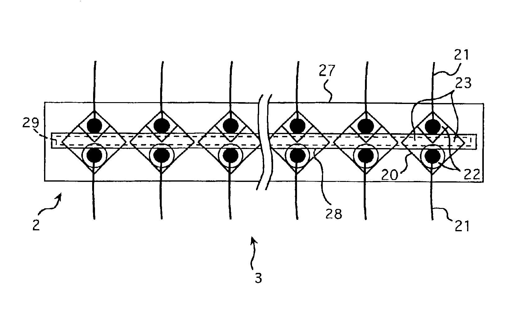
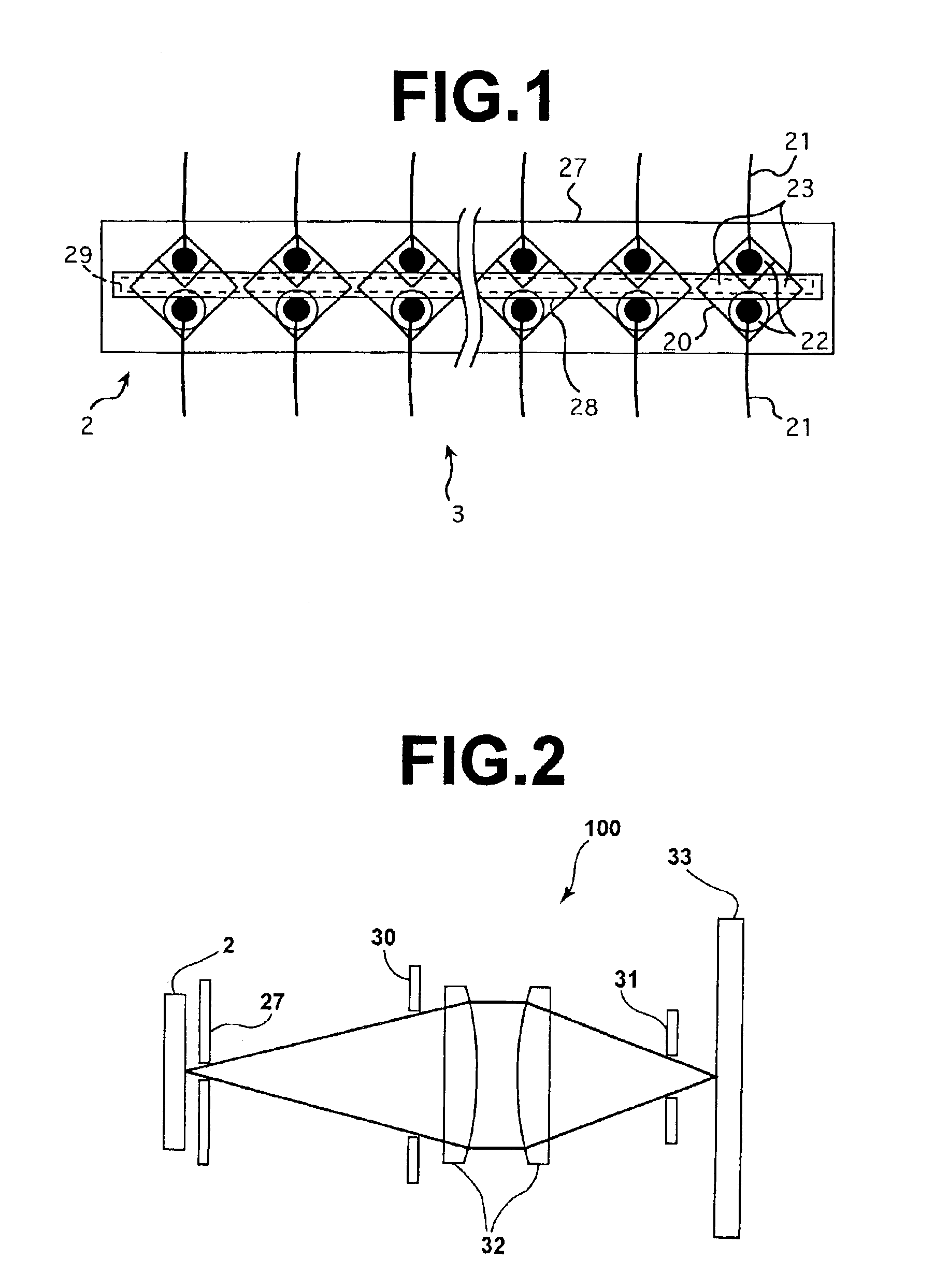
[0040]First, preferred embodiments of a linear light source according to the invention will be described hereinafter. FIG. 1 is a schematic configuration diagram of a linear light source 3 according to the invention. In FIG. 1, the linear light source 3 comprises a light source 2 having a plurality of LED chips 20 disposed in a straight line and a slit 27 having an opening 28 extending in the longitudinal direction of the light source 2.

[0041]The LED chip 20 has bonding pad sections 22 for direct bonding of wires to the electrodes of the chip and emission regions 23 which emit light when a current flows between the electrodes, and the boding pad sections 22 are connected to a power supply (not shown) through an Au wire 21. The slit 27 is finished in matte-black and is insulated.

[0042]Each of the LED chips 20 is disposed in such a way that its emission regions 23 along a diagonal line are aligned with those of adjacent LED chips in a straight line. The slit 27 is disposed in such a w...

second embodiment

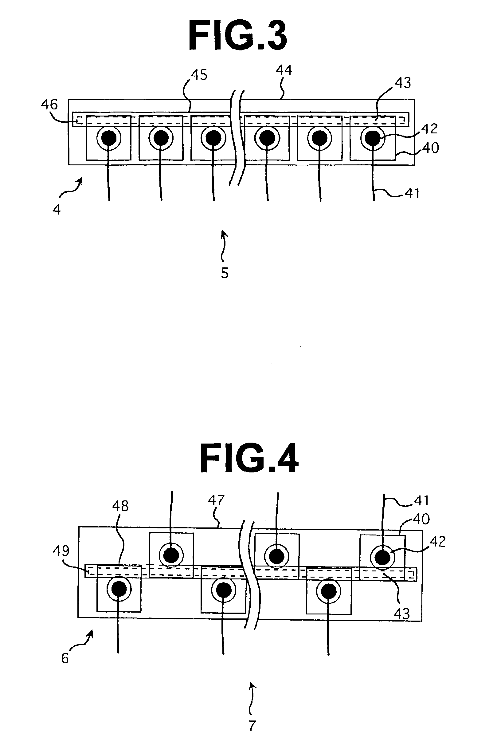
[0051]FIG. 3 is a schematic configuration diagram of a linear light source 5 according to the invention. The linear light source 5 comprises a light source 4 and a slit 44 having an opening 45 extending in the longitudinal direction of the light source 4. The light source 4 comprises a plurality of LED chips 40, each having a bonding pad section 42, which is a non-emission region, in the center and emission region 43 in the periphery, disposed adjacently in such a way that the bonding pad sections 42 are aligned in a straight line. All Au wires 41 connected to the bonding pad sections 42 of the respective LED chips 40 are extended in the same direction substantially perpendicular to the arranging direction of the LED chips 40. The slit 44 is disposed in such a way that the opening 45 of the slit 44 is placed opposite to the emission regions 43 located on the opposite side of the wires.

[0052]A utilization area 46 is defined by the opening 45 of the slit 44. The utilization area 46 in...

fifth embodiment

[0063]Next, FIG. 7 is a schematic configuration diagram of an electroradiographic detection / reading system based on the reading light exposure apparatus 100 according to the invention. FIG. 7A is a perspective view and FIG. 7B is an X-Z cross-sectional view thereof. As shown in FIG. 7, the system comprises an electrophotographic recording medium 60 formed on a glass substrate 66; an exposure apparatus for radiating reading light onto the electrophotographic recording medium 60 when reading out image information from the medium 60; and an electric current detection means 50 for detecting a current flowing out from the medium 60 produced by the scanning of the medium 60 with the reading light.

[0064]The electrophotographic medium, which is an electroradiographic medium, records electroradiographic information as an electrophotographic latent image and produces an electric current in accordance with the electrophotographic latent image. More specifically, it is a multi-layered medium co...


PUM


Abstract

A linear light source has LED chips disposed in an array that provides a higher-intensity light beam with a narrower half-beam width at the converging point. Each of the LED chips is disposed in such a way that its emission regions along a diagonal line are aligned with those of adjacent chips in a straight line. The slit is disposed in such a way that its opening is placed opposite to the emission regions aligned in a straight line. The utilization area is defined by the opening of the slit. The utilization area can include a larger emission region than that of the conventional linear light source so that a higher-intensity light beam with a narrower half-beam width can be obtained at the converging point.

Description

BACKGROUND OF THE INVENTION[0001]1. Field of the Invention[0002]The present invention relates to a linear light source. More specifically, it is directed to a linear light source comprising a plurality of luminous elements disposed in a straight line, and an apparatus capable of radiating reading light onto image recording media to read out images recorded thereon using said light source.[0003]2. Description of the Related Art[0004]In medical X-ray photography, an image reading system for reading out an electrophotografic latent image or electroradiographic image information has been proposed, in which a photoconductor made of an X-ray sensitive material, such as an a-Se selenium plate, is used as an electrophotografic recording medium to reduce an amount of dosage exposed to a subject and to improve diagnostic accuracy, and a radial ray, such as an X-ray which carries electroradiographic image information is radiated onto the medium to store charges of a latent image carrying the e...

Claims


Application Information

Patent Timeline
IPC IPC(8): H01L25/075G03B42/02H01L33/38H01L33/50H01L33/62H04N1/028H04N1/04
CPCG03G15/054H01L25/0753H01L2924/3025H01L2924/00H01L2224/48463H01L2224/49175H01L2224/45144H01L2924/16151H01L2924/16195
Inventor HAKAMATA, KAZUO
Owner FUJIFILM CORP
Why Eureka
Try Eureka