Method for inspection of periodic grating structures on lithography masks

a lithography mask and periodic grating technology, applied in the field of masks, can solve the problems of systematic manufacturing faults, unsatisfactory brightness errors, and local properties defects of lithography masks, and achieve the effects of convenient compensation, less stringent requirements, and improved sensitivity

Inactive Publication Date: 2007-08-28
QIMONDA
View PDF9 Cites 3 Cited by
  • Summary
  • Abstract
  • Description
  • Claims
  • Application Information

AI Technical Summary

Benefits of technology

[0027]The only disadvantage of this method is that a restriction to periodic structures is necessary. It should be remembered, however, that the r

Problems solved by technology

Global properties are, for example, the error in the line width (CD target value) from the target size (offset error), as well as the fluctuation in the error over the image area (uniformity error).
Undesirable brightness errors occur due to discrepancies from the ideal etching depth, and these likewise represent a global mask property.
Local properties are defects on the mask which occur either due to faults in the production of the mask or due to subsequent impurities, e.g., dust.
At present, systematic manufacturing faults in lithography masks such as regular errors in the line separation (offset target error) and changes in the line width (uniformity error) are measured directly on the structures by means of different SEM measurements (Scanning Electron Microscopy) at a large number of points on the mask.
However, this is a time-consuming and unreliable assessment process, since the measurement errors and the poor reproducibility of SEM measurements are disadvantageous.
For this reason, this method is not suitable for lithography masks which are etched in quartz, since there are no well-defined etchings for SEM measurement in masks such as these.
Mask assessment for new mask technologies, such as interference masks, is very difficult.
However, no known method exists for determination of the diffraction and transmission parameters.
Since each process step

Method used


Image

  • Method for inspection of periodic grating structures on lithography masks
  • Method for inspection of periodic grating structures on lithography masks
  • Method for inspection of periodic grating structures on lithography masks

Examples


Embodiment Construction

[0044]The making and using of the presently preferred embodiments are discussed in detail below. It should be appreciated, however, that the present invention provides many applicable inventive concepts that can be embodied in a wide variety of specific contexts. The specific embodiments discussed are merely illustrative of specific ways to make and use the invention, and do not limit the scope of the invention.

[0045]Various embodiments of the present invention will now be described. After a written description, specific examples will be described with respect to the Figures.

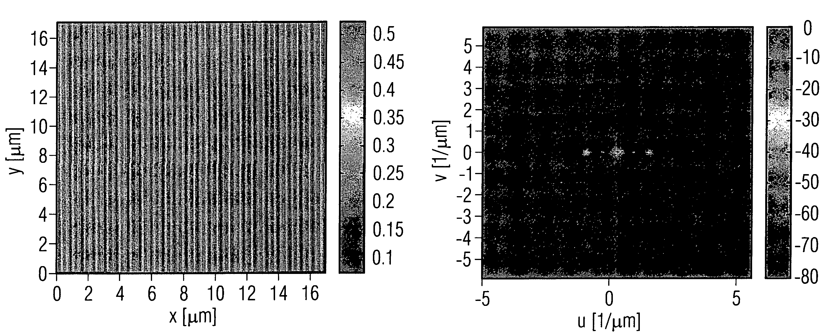
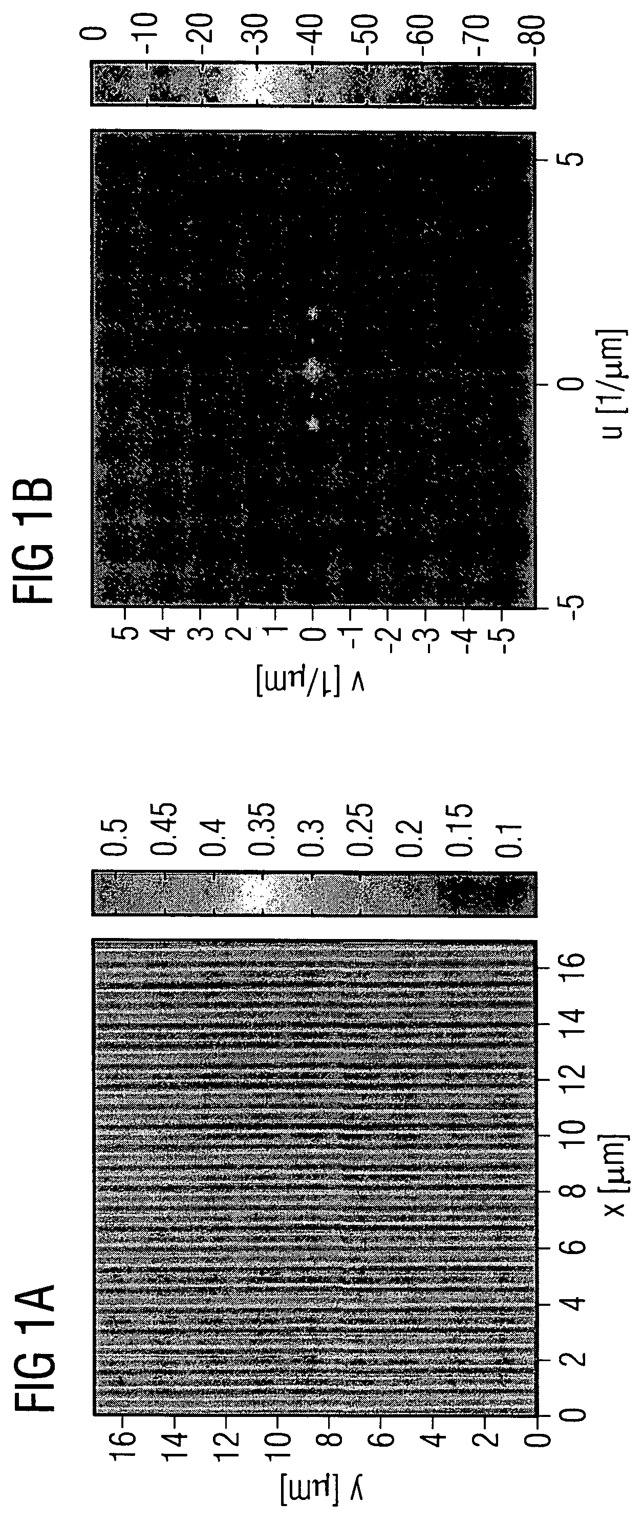
[0046]In a first aspect, the present invention provides for the calibration of a first image of each array structure for selected locations on the lithography mask, calculation of the Fourier coefficients at a reference point of an array / diffraction grating, calculation of a residual image from a difference between an original image of the array structure and Fourier expansion, and formation of a threshold value...


PUM


Abstract

The invention relates to a method for inspection of periodic structures on lithography masks using a microscope with adjustable illumination and an operating element for movement of a mechanical stage with the lithography mask attached to it in order to record images of the lithography mask at a computer-controlled location on the lithography mask. The position, the size and the pitch specification of the lithography mask are stored.

Description

TECHNICAL FIELD[0001]The present invention relates generally to masks and, more preferably, to a method for inspection of periodic grating structures on lithography masks.BACKGROUND[0002]As is known in microlithography, semiconductor structures are produced by the imaging of a structure which has previously been produced on a lithography mask on a wafer that is coated with a photoresist and by exposure and subsequent development of the photoresist.[0003]After the manufacture of the lithography mask, the mask has different properties, which vary from mask to mask. These different properties have a considerable influence on photolithography and on the imaging thereof. In this case, a distinction is drawn between general (global) and local properties which are normally specified.[0004]Global properties are, for example, the error in the line width (CD target value) from the target size (offset error), as well as the fluctuation in the error over the image area (uniformity error). In al...

Claims


Application Information

Patent Timeline
IPC IPC(8): G01B11/00G03F1/00G03F7/40
CPCG01N21/95623G03F1/84G06T7/001G01N2021/95676G06T2207/10056G06T2207/30148
Inventor DETTMANN, WOLFGANGKOEHLE, RODERICKVERBEEK, MARTIN
Owner QIMONDA
Why Eureka
Try Eureka