Device architecture and process for improved vertical memory arrays

a technology of vertical memory array and device architecture, applied in the field of integrated circuit architecture, can solve the problems that conventional diagnostic structures may not be suited for measuring such vm arrays

Inactive Publication Date: 2005-08-16
POLARIS INNOVATIONS
View PDF4 Cites 99 Cited by
  • Summary
  • Abstract
  • Description
  • Claims
  • Application Information

AI Technical Summary

Benefits of technology

[0009]An integrated circuit for testing performance of memory devices composed of an array of memory cells which each include a vertical FET access transistor and a deep trench capacitor is also disclosed. The integrated circuit also contains a series of parallel wordlines, a series of parallel bitlines, a buried drain contact strip that connects a bitline to a memory cell, and a test structure comprise of at least one pair of c

Problems solved by technology

In memory arrays based on vertical access transistors and vertical trenches as described above (VM), the fabrication proces

Method used


Image

  • Device architecture and process for improved vertical memory arrays
  • Device architecture and process for improved vertical memory arrays
  • Device architecture and process for improved vertical memory arrays

Examples


Embodiment Construction

[0015]The following list of symbols is used consistently throughout the text and drawings.

List of Reference Symbols

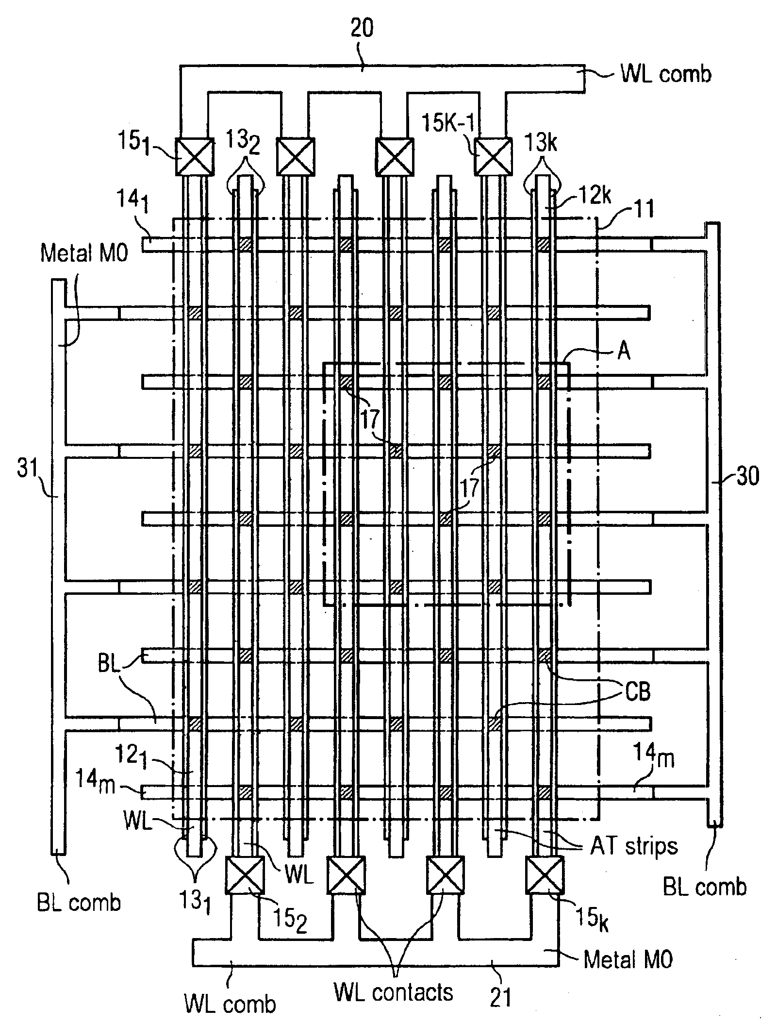
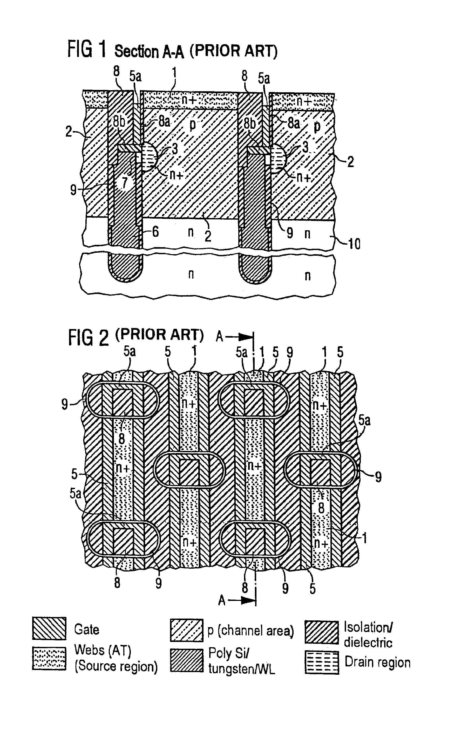
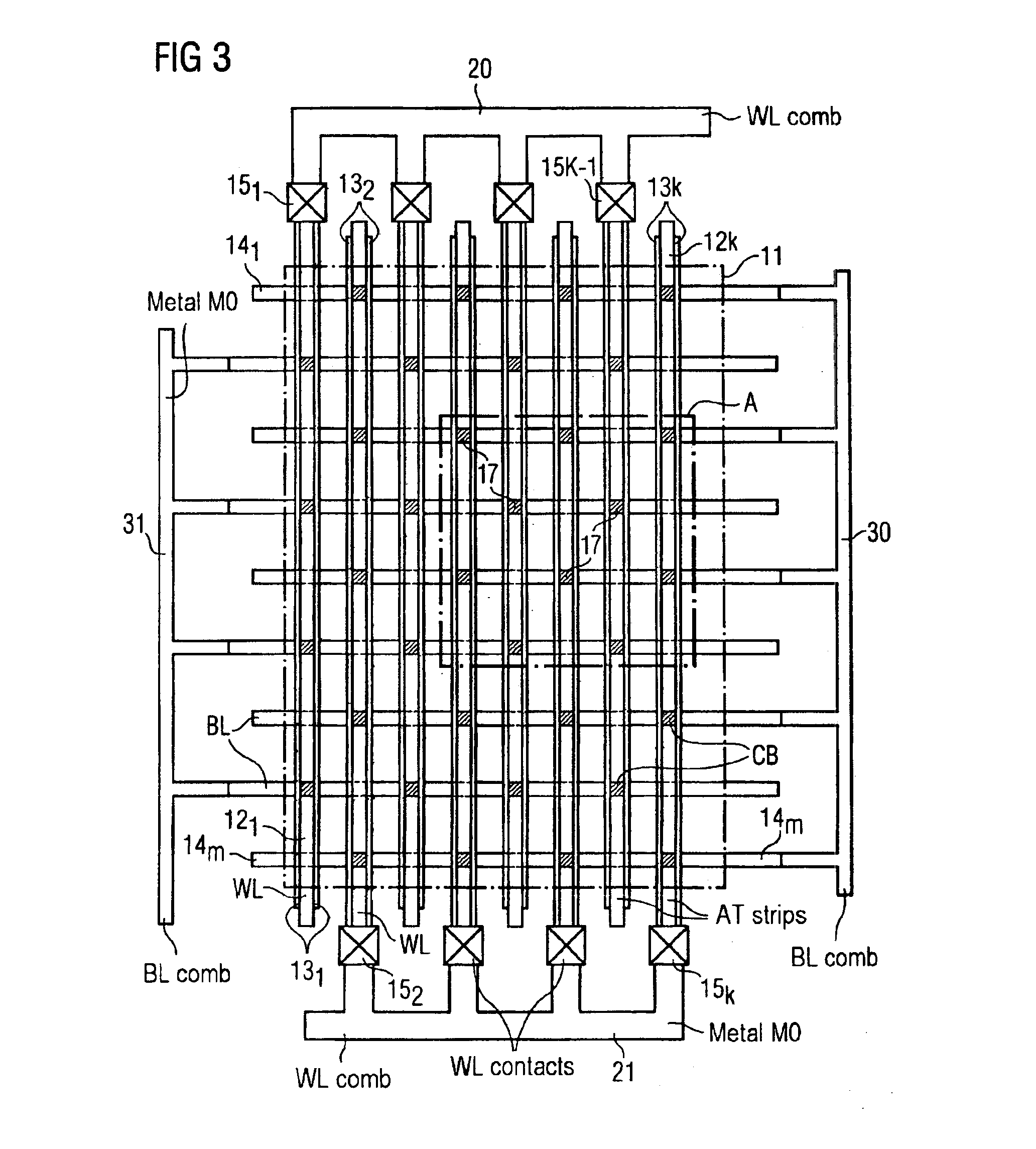
[0016]1 Drain electrode[0017]2 Channel zone[0018]3 Source electrode[0019]4 Bulk[0020]5, 5A Gate electrode strips[0021]6 Polysilicon column[0022]7 Contact between the source electrode and the polysilicon column[0023]8, 8A, 8B, 9 Isolation / dielectric[0024]10 Substrate[0025]11 FET transistor array[0026]12 AT strip[0027]13 Word lines[0028]14 Bit lines[0029]15 Word line contacts[0030]17 Contacts with the bit line (CB)[0031]18 Buried drain contact strip[0032]20, 21 First, second word line comb[0033]24 Metal M0[0034]25 Word line meander[0035]30, 31 First and second bit line comb[0036]35 Bit line meander[0037]40 Transistor formed by the buried drain contact strip 18

[0038]Before describing in detail embodiments of the present invention including an integrated circuit and array process diagnosis test structure integrated therein, in the following text, a known concept of a transi...


PUM


Abstract

An array process diagnosis test structure for an integrated circuit including a transistor array composed of vertical FET memory cell access transistors, which are formed into the depth of a substrate in the form of active webs which run parallel in the lateral direction of the circuit is disclosed. Memory cell storage capacitors in the array test structure are formed in deep trenches on the end faces of those sections of the active webs which form the vertical FET transistors. Word lines are arranged along the webs and along parallel intersecting bit lines of the array, outside of which, and on two mutually opposite edges, are located a first and second word line comb. The wordline combs are offset and connected alternately to different word lines. In addition, a first and a second bit line comb are formed on the two other opposing edges of the transistor array mutually offset and each connected to different bit lines. The test structure provides a convenient means to carry out reliability investigations on the gate oxide of the vertical FET transistors and on the capacitor dielectric in the deep trenches, capacitance measurements between the word lines, and between the word lines and other circuit layers, as well as capacitance measurements between the bit lines and between the bit lines and other circuit layers, and thus facilitates diagnosis of possible fault sources arising during the production process.

Description

BACKGROUND[0001]1. Field of the Invention[0002]The present invention relates generally to integrated circuit architecture and more particularly to memory arrays.[0003]2. Background of the Invention[0004]The continuing trend of size reduction of semiconductor memory components in products such as dynamic random access memory (DRAM) has led to development of vertical trench storage capacitors and more recently, vertical access transistors. Both of these devices are associated with the basic unit of a DRAM, the memory cell. An example of a DRAM cell based on a vertical access transistor is disclosed in U.S. Pat. No. 5,519,236. Use of a vertical trench capacitor and a vertical access transistor facilitates the fabrication of a semiconductor memory cell where F=70 nm or less, while at the same time making it possible to maintain the performance of the access transistor.[0005]In order to fabricate the above-described structures, parallel-running active webs that are filled with silicon ar...

Claims


Application Information

Patent Timeline
IPC IPC(8): H01L23/544G11C29/02H01L21/8242H01L27/02H01L27/108
CPCG11C29/02G11C29/025H01L22/34H01L27/0207H01L27/10841H01L27/10882H01L27/10885H01L27/10891G11C2029/5002Y10S257/908H10B12/395H10B12/48H10B12/488H10B12/482
Inventor KOWALSKI, BERNHARDFELBER, ANDREASROSSKOPF, VALENTINSCHLOESSER, TILLLINDOLF, JUERGEN
Owner POLARIS INNOVATIONS
Why Eureka
Try Eureka