Unlock instant, AI-driven research and patent intelligence for your innovation.

Jitter measuring system in high speed data output device and total jitter measuring method

a data output device and jitter measurement technology, applied in the field of jitter measurement system and total jitter measurement method in high-speed data output device, can solve the problems of noise generated during the operation of an integrated circuit, cost increase, error or data loss, etc., and achieve the effect of short time and high cos

Inactive Publication Date: 2005-08-16
SAMSUNG ELECTRONICS CO LTD
View PDF8 Cites 2 Cited by
  • Summary
  • Abstract
  • Description
  • Claims
  • Application Information

AI Technical Summary

Benefits of technology

[0010]It is therefore an object of the present invention to provide a jitter measuring system and method, which are capable of addressing the limitations of the conventional approaches.
[0012]Another object of the present invention is to provide an improved jitter measuring system and a total jitter measuring method therefor, which is capable of measuring total jitter of high speed data at a rate of over 2.0 Gbps, in a comparatively short time period.
[0013]An additional object of the present invention is to provide a total jitter measuring method, in which even data dependent jitter (DDJ), which is an important influence on total jitter characteristics, can be accurately measured.
[0019]Such systematic and methodic construction allows for measurement of the total jitter of the high speed data output in a relatively short time without the need for employing a high cost measuring instrument.

Problems solved by technology

In general, jitter generated during operation of an integrated circuit is a type of noise.
It is well known that such jitter can cause an error, or data loss, during operation.
For this and other reasons, there is a problem with cost increase due to the additional installation of the measuring instrument, and of a increase in time consumed by the test in gaining the result through the test device.

Method used


Image

  • Jitter measuring system in high speed data output device and total jitter measuring method
  • Jitter measuring system in high speed data output device and total jitter measuring method
  • Jitter measuring system in high speed data output device and total jitter measuring method

Examples


Embodiment Construction

[0027]Hereinafter, preferred embodiments of the present invention will be described in detail with reference to the accompanying drawings.

[0028]In accordance with the preferred embodiments of the present invention, a jitter measuring system in a high speed data output device and a total jitter measuring method will be described with the same or similar reference characters and numbers for constructive elements which have the same or similar functions even, on mutually different drawings.

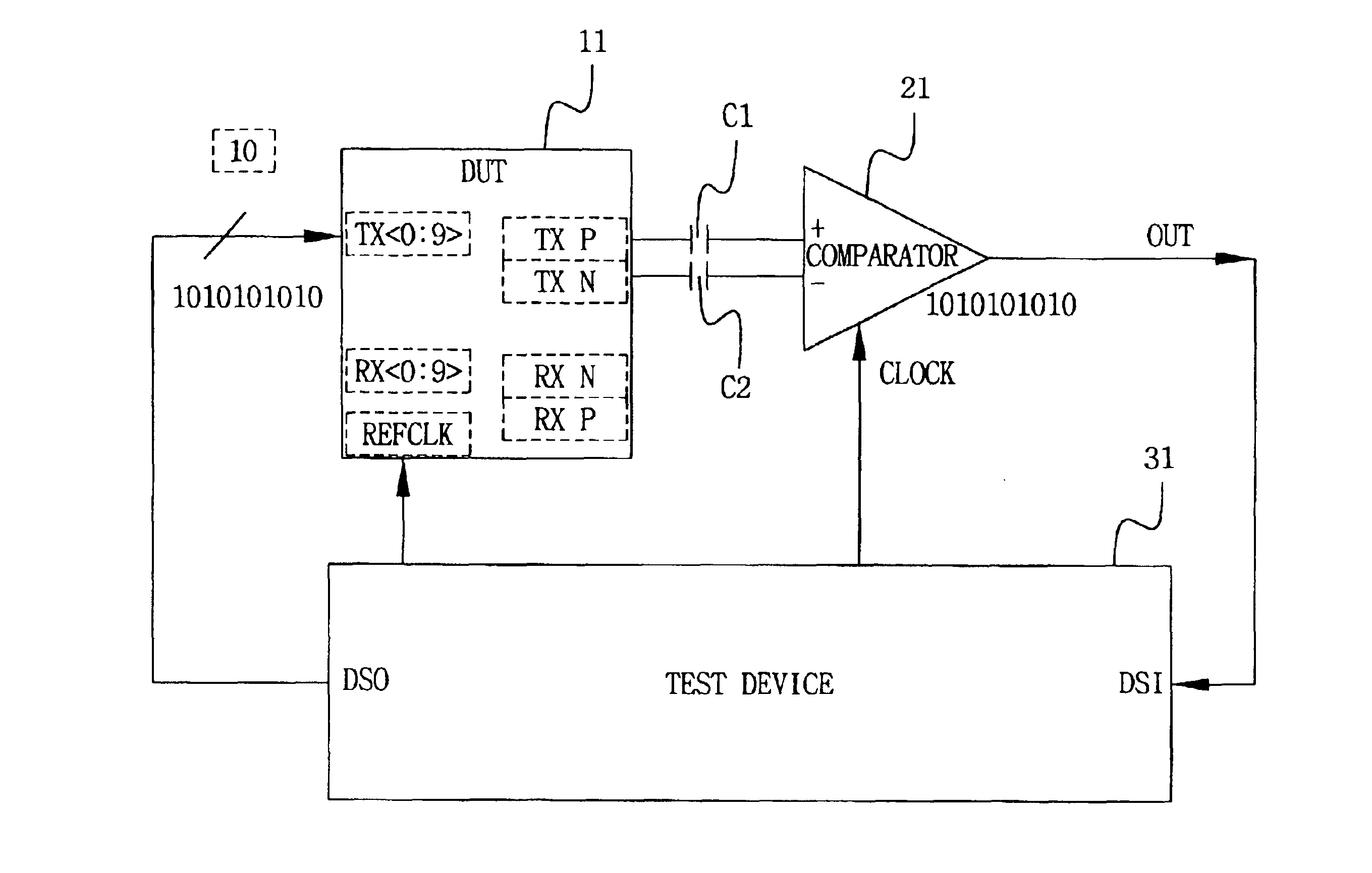
[0029]FIG. 2 is a block diagram of a jitter measuring system according to an embodiment of the present invention. FIG. 3 is a schematic diagram of a detailed connection in relation to the comparator of FIG. 2. FIGS. 2 and 3 provide the construction of the jitter measuring system using a high speed comparator without the need for employing the conventional measuring instrument 20. A high speed data output device DUT 11 as the tested object is connected to a test device 31 for providing testing data DS...


PUM


Abstract

In a system and method for measuring total litter in a high speed data processing device, a high-speed data processing device, as an object under test, receives test data and generates differential output data at a high rate. A test device provides the test data to the high speed data processing device and provides a comparison operation reference clock. A high-speed differential comparator is coupled between the high speed data processing device and the test device for comparing the differential output data of the high speed data processing device in response to the comparison operation reference clock. In this manner, measurement of total jitter in a high speed data processing device can be achieved rapidly and without the need for employing a high-cost measuring instrument.

Description

BACKGROUND OF THE INVENTION[0001]1. Field of the Invention[0002]The present invention relates to testing of semiconductor devices, and more particularly, to a jitter measuring system and a total jitter measuring method in a high speed data output device.[0003]2. Prior Art of the Invention[0004]In general, jitter generated during operation of an integrated circuit is a type of noise. It is well known that such jitter can cause an error, or data loss, during operation. For this reason, accurate measurement of jitter generated in an integrated circuit device is desired.[0005]In a high speed data processing device having a data speed on the order of 1 GHz or greater, e.g., a parallel / serial converter etc., in the case where total jitter of output data is measured by automated test equipment (ATE), it is highly desired during testing that jitter be measured to high accuracy. The total jitter of a system can be categorized into “DJ” (Deterministic Jitter) and “RJ” (Random Jitter). DJ jitt...

Claims


Application Information

Patent Timeline
IPC IPC(8): G01R29/02G01R31/319G01R31/28G06F11/30G06F15/00H04L25/02G01R31/317G06F11/24
CPCG01R31/31725G06F11/24G01R31/28
Inventor JANG, JIN-MO
Owner SAMSUNG ELECTRONICS CO LTD