System and method for designing dynamic circuits in a SOI process

a dynamic circuit and soi technology, applied in the direction of program control, pulse technique, instruments, etc., can solve the problems of reducing the design efficiency of dynamic circuits, affecting the switching speed, and contributing to the added power consumption

Inactive Publication Date: 2005-08-16
SAMSUNG ELECTRONICS CO LTD
View PDF13 Cites 11 Cited by
  • Summary
  • Abstract
  • Description
  • Claims
  • Application Information

AI Technical Summary

Benefits of technology

[0006]The present invention is directed to a system and method for designing a dynamic circuit in a silicon-on-insulator (SOI) process comprising the steps of representing the dynamic circuit using at least one logic circuit, wherein the at least one logic circuit is sel

Problems solved by technology

This capacitance not only delays the switching speed, but also contributes to added power consumption.
The f

Method used


Image

  • System and method for designing dynamic circuits in a SOI process
  • System and method for designing dynamic circuits in a SOI process
  • System and method for designing dynamic circuits in a SOI process

Examples


Embodiment Construction

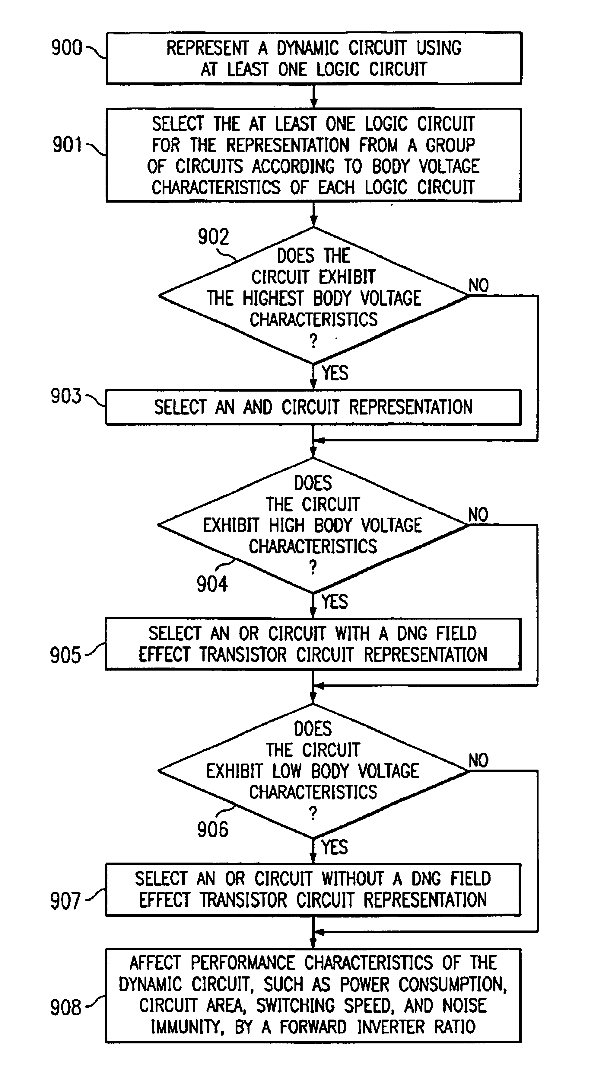
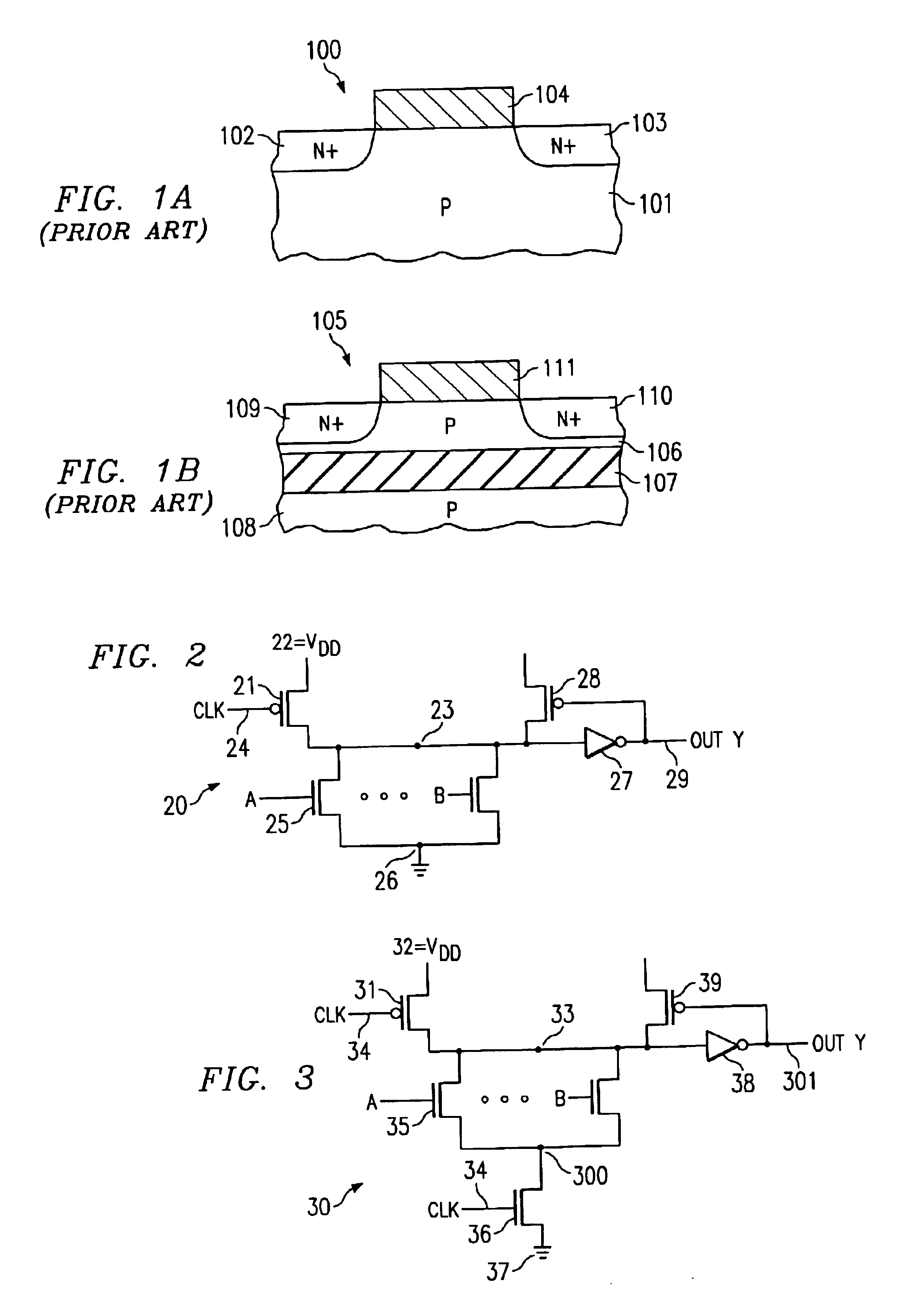
[0019]Dynamic circuits typically are constructed with similar basic parts. FIG. 2 is a circuit diagram representation of an OR logic circuit in accordance with an embodiment of the present invention. While FIG. 2 shows one of the circuits used in design methodologies implemented according to the teachings of the present invention, it is also configured as a simple dynamic circuit. OR circuit 20 may comprise one FET positioned to assist in charging storage node 23 to the appropriate / desired charge / value. This FET is generally referred to as “pre-charge” FET 21. Another typical feature of a dynamic circuit, such as OR circuit 20, is another FET positioned to hold the storage node 23 at the desired charge / value. This FET is generally referred to as “holder” FET 28 and may be either a p- or n-type FET (typically a p-type, PFET) depending on the configuration of the overall circuit technology. Because of their typical configuration, pre-charge FET 21 will generally be the same type (p- o...


PUM


Abstract

A system and method is disclosed for designing a dynamic circuit in a silicon-on-insulator (SOI) process comprising the steps of representing the dynamic circuit using at least one logic circuit, wherein the at least one logic circuit is selected from a group consisting of: an OR circuit with a DNG field effect transistor (FET), an OR circuit, and an AND circuit, and wherein the at least one logic circuit is selected according to body voltage characteristics of each circuit in the group.

Description

RELATED APPLICATIONS[0001]This application is related to concurrently filed and commonly assigned U.S. patent application Ser. No. 10 / 282,478 entitled “PROCESS AND SYSTEM FOR DEVELOPING DYNAMIC CIRCUIT GUIDELINES”, the disclosure of which is hereby incorporated herein by reference.FIELD OF THE INVENTION[0002]The present invention is directed to designing dynamic circuits and, more specifically, to a system and method for representing all silicon-on-insulator (SOI)-based dynamic circuits via a combination of, at most, three logic circuits.BACKGROUND[0003]Dynamic circuits are circuits designed for high speed logic gates. The intent for such circuits is typically to achieve the fastest switching speed available with the lowest possible power consumption. Dynamic circuits have been implemented in bulk complementary metal-oxide semiconductor (CMOS) in order to take advantage of the speed and power benefits of CMOS. Recent advances in integrated circuit technology have shown the speed and...

Claims


Application Information

Patent Timeline
IPC IPC(8): G06F17/50H01L21/822H01L21/82H01L27/04H01L27/12H03K19/096
CPCG06F17/5045G06F30/30
Inventor GUNDERSON, JASON R.LACHMAN, JONATHAN E.MCFARLAND, ROBERT
Owner SAMSUNG ELECTRONICS CO LTD
Why Eureka
Try Eureka