Method of forming film

Inactive Publication Date: 2005-08-23
TOKYO ELECTRON LTD
View PDF5 Cites 5 Cited by
  • Summary
  • Abstract
  • Description
  • Claims
  • Application Information

AI Technical Summary

Benefits of technology

[0013]According to the present invention, it is possible to change the discharge direction of the coating solution to the outer peripheral portion of the substrate, thereby reducing the amount of application to the outer peripheral portion of the substrate, so that it is possible to restrain protuberance of the coating solution at the outer peripheral portion of the substrate caused by surface tension. Consequently, a uniform coating film is formed also at the outer peripheral portion on the substrate, and thus a region on the substrate which can be used as products is increased in area to improve yields.
[0014]The discharge direction of the coating solution is changed only when the coating solution discharge member moves from the inside to the outside of the substrate to thereby cross the outer peripheral portion of the substrate or when it reversely moves from the outside to the inside of the substrate to thereby cross the outer peripheral portion of the substrate, whereby the discharge is performed, as a result, only when the coating solution discharge member moves in one direction, so that the amount of application to the outer peripheral portion of the substrate is reduced to half. Accordingly, protuberance at the outer peripheral portion is restrained to thereby improve yields. Moreover, the amount of application can be reduced correspondingly, resulting in reduced cost.

Problems solved by technology

However, in the spin coating method, since the wafer is rotated at high speed, a large amount of resist solution scatters from the peripheral portion of the wafer, resulting in a big waste of resist solution.
Further, the apparatus is contaminated by the scatter of the resist solution, bringing about harmful effects such as a need for cleaning frequently.
However, in the case in which the resist solution is applied in the manner of the so-called single stroke, it is feared that the resist solution applied at the peripheral portion of the wafer protrudes by surface tension, with the result that a resist film is not uniformly formed.
When exposure is performed with the resist film protruding at the peripheral portion, the peripheral portion becomes a defective portion which can not be used as products, whereby yields correspondingly decrease.

Method used


Image

  • Method of forming film
  • Method of forming film
  • Method of forming film

Examples


Embodiment Construction

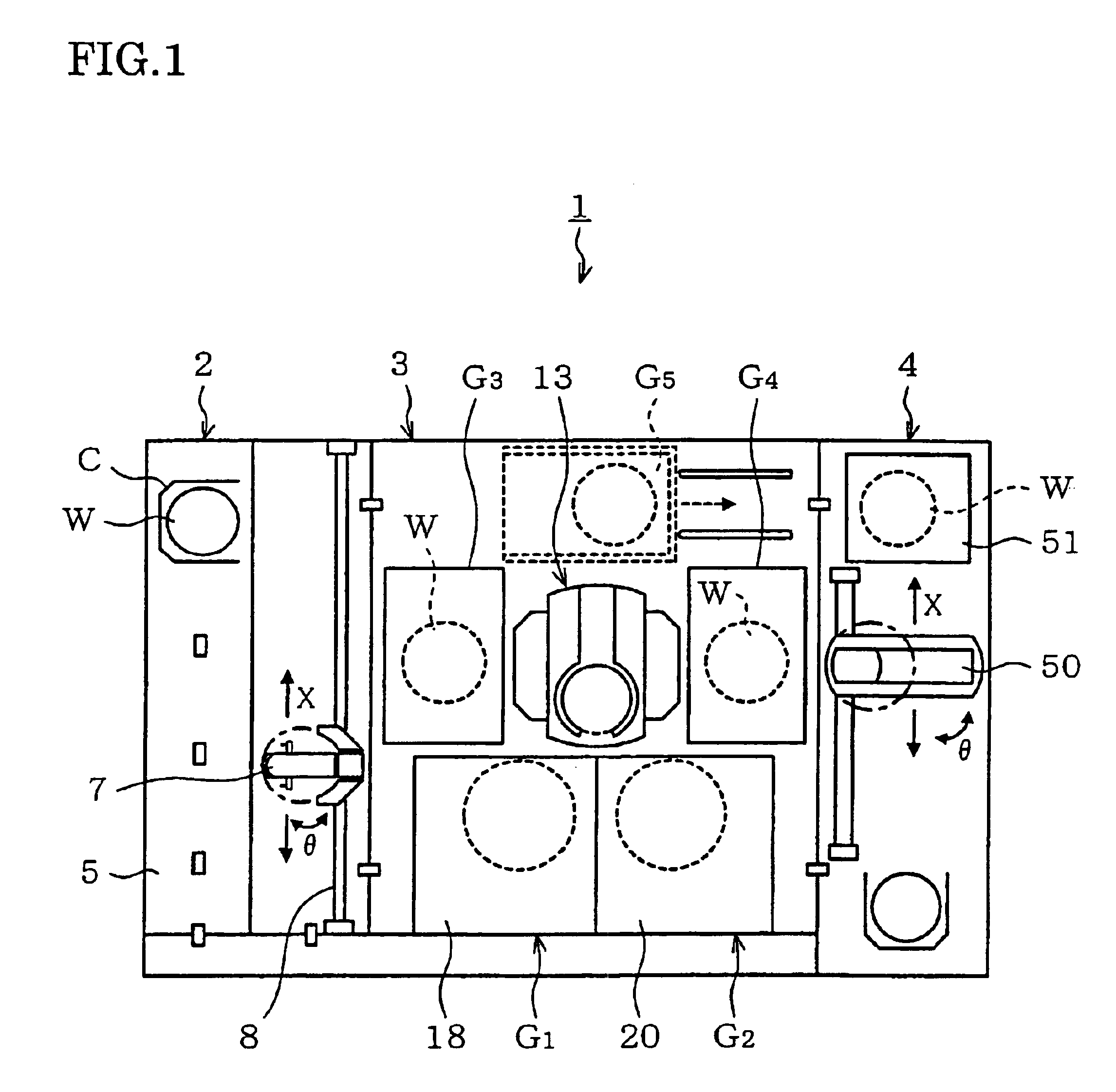
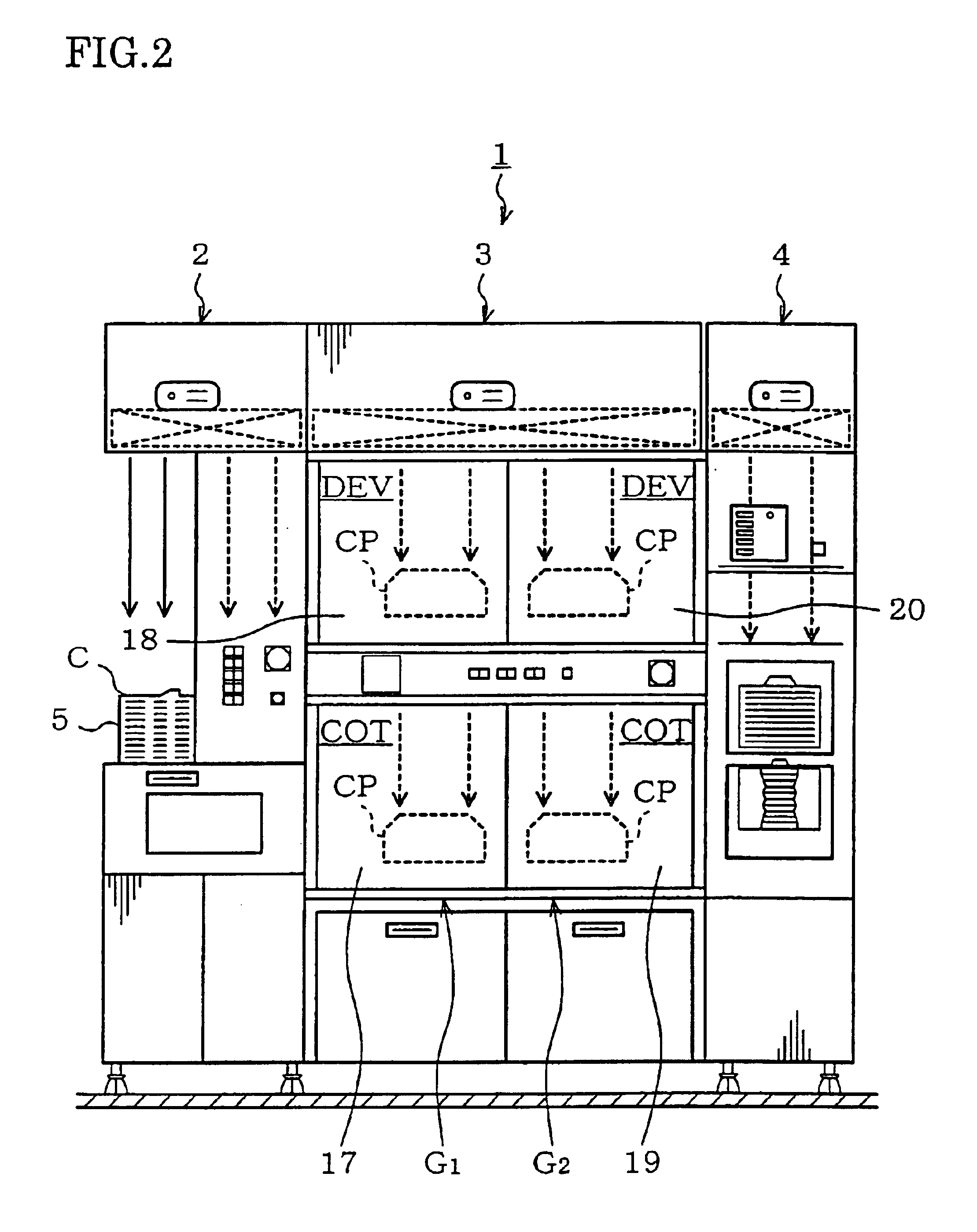
[0032]Hereinafter, preferable embodiments of the present invention will be described. FIG. 1 is a plan view of a coating and developing system 1 including a resist coating unit according to an embodiment, FIG. 2 is a front view of the coating and developing system 1, and FIG. 3 is a rear view of the coating and developing system 1.

[0033]The coating and developing system 1 has a configuration, as shown in FIG. 1, in which a cassette station 2 for carrying, for example, 25 wafers W, as a unit of cassette, from / to the outside into / out of the coating and developing system 1 and carrying the wafer W into / out of a cassette C, a processing station 3 in which various kinds of processing and treatment units each for performing predetermined processing or treatment for the wafers W one by one in coating and developing steps are multi-tiered, and an interface section 4 for delivering the wafer W to / from a light-exposure apparatus (not shown) provided adjacent to the processing station 3 are in...


PUM

PropertyMeasurementUnit
Surface tensionaaaaaaaaaa

Abstract

A method of forming a film of a coating solution on a substrate includes steps of moving a coating solution discharge member relative to a substrate while a coating solution is being discharged from the coating solution discharge member to the surface of the substrate, and changing a discharge direction of the coating solution to an outer peripheral portion of the substrate to make the amount of application to the outer peripheral portion smaller than that to other portions. This can reduce the amount of application to the outer peripheral portion of the substrate, thereby making it possible to restrain protuberance of the coating solution at the outer peripheral portion of the substrate caused by surface tension. Consequently, a coating film which is uniform also at the outer peripheral portion on the substrate is formed.

Description

CROSS-REFERENCE TO RELATED APPLICATIONS[0001]This application is based upon and claims the benefit of priority from the prior Japanese Patent Application No. 11-328800, filed Nov. 18, 1999, and is a divisional application of U.S. patent application Ser. No. 09 / 712,179, filed Nov. 15, 2000, now U.S. Pat. No. 6,537,373 the entire contents of which are incorporated herein by reference.BACKGROUND OF THE INVENTION[0002]The present invention relates to a method of forming a film on a substrate and an apparatus thereof.[0003]In a photolithography process in the semiconductor device fabrication processes, for example, resist coating treatment in which a resist solution is applied to the surface of a wafer to form a resist film, exposure processing in which the wafer is exposed in a pattern, developing treatment in which development is performed for the exposed wafer, and the like are performed to form a predetermined circuit pattern on the wafer.[0004]At present, in the above-described resi...

Claims


Application Information

Patent Timeline
IPC IPC(8): G03F7/16H01L21/00B05D1/00B05B15/04B05C5/00B05C13/02B05D1/30H01L21/027
CPCG03F7/162H01L21/6715B05D1/005H01L21/027
Inventor KITANO, TAKAHIROKOBAYASHI, SHINJIESAKI, YUKIHIKOMORIKAWA, MASATERU
Owner TOKYO ELECTRON LTD
Why Eureka
Try Eureka