

Semiconductor device and method of manufacturing the same
- Summary
- Abstract
- Description
- Claims
- Application Information
AI Technical Summary
Benefits of technology
Problems solved by technology
Method used
Image

Examples
Embodiment Construction
[0062]The First Preferred Embodiment
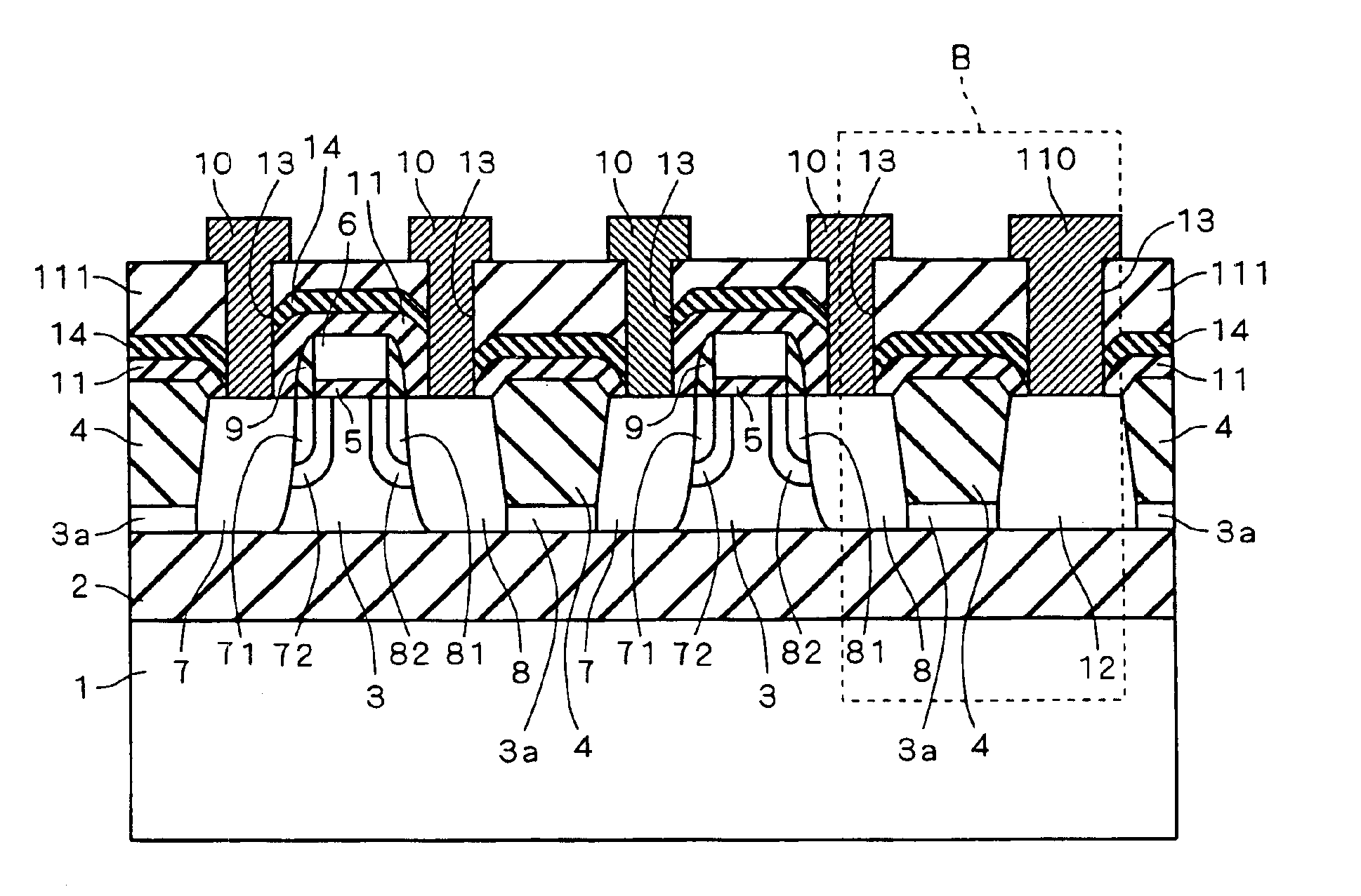
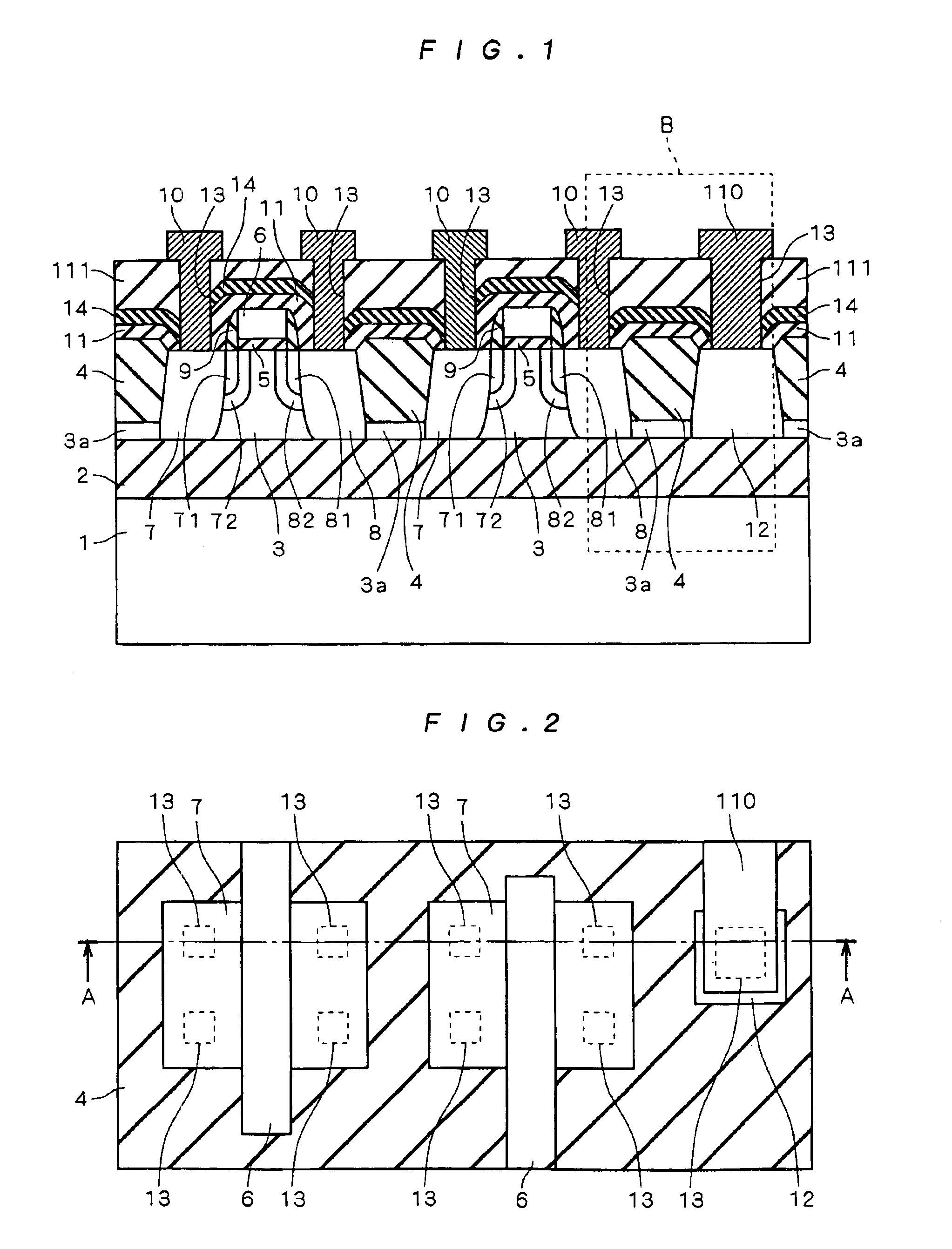
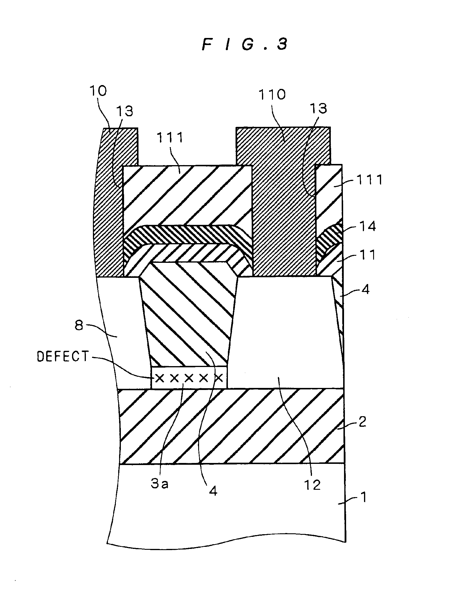
[0063]FIG. 1 is a cross section showing a semiconductor device in accordance with the first preferred embodiment of the present invention. The semiconductor device of FIG. 1 comprises a semiconductor substrate 1, a buried oxide film 2, a semiconductor layer 3, an isolation insulating film 4, a gate insulating film 5, a gate electrode 6, source / drain regions 7, 71, 8, and 81, pocket implantation regions 72 and 82, a sidewall insulating film 9, wires 10 and 110, interlayer insulating films 11 and 111, a p-type impurity region 12, a contact hole 13 and a silicon nitride film 14. Further, the semiconductor layer 3 (the first semiconductor region) below the isolation insulating film 4 is particularly represented as 3a.
[0064]FIG. 2 is a plan view showing the semiconductor device in accordance with the first preferred embodiment of the present invention. FIG. 1 is the cross section taken along the section A—A of FIG. 2. In FIG. 2, the interlayer insulat...
PUM
 Abstract
Description
Claims
Application Information