

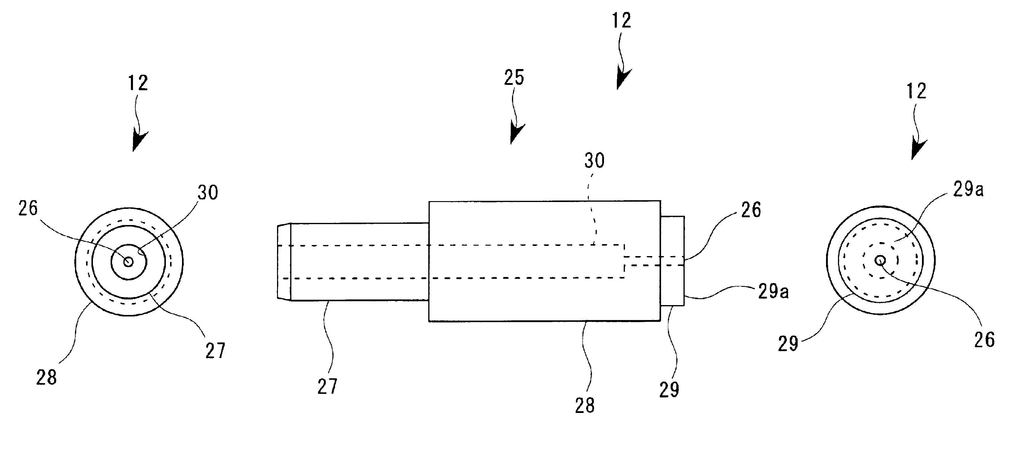
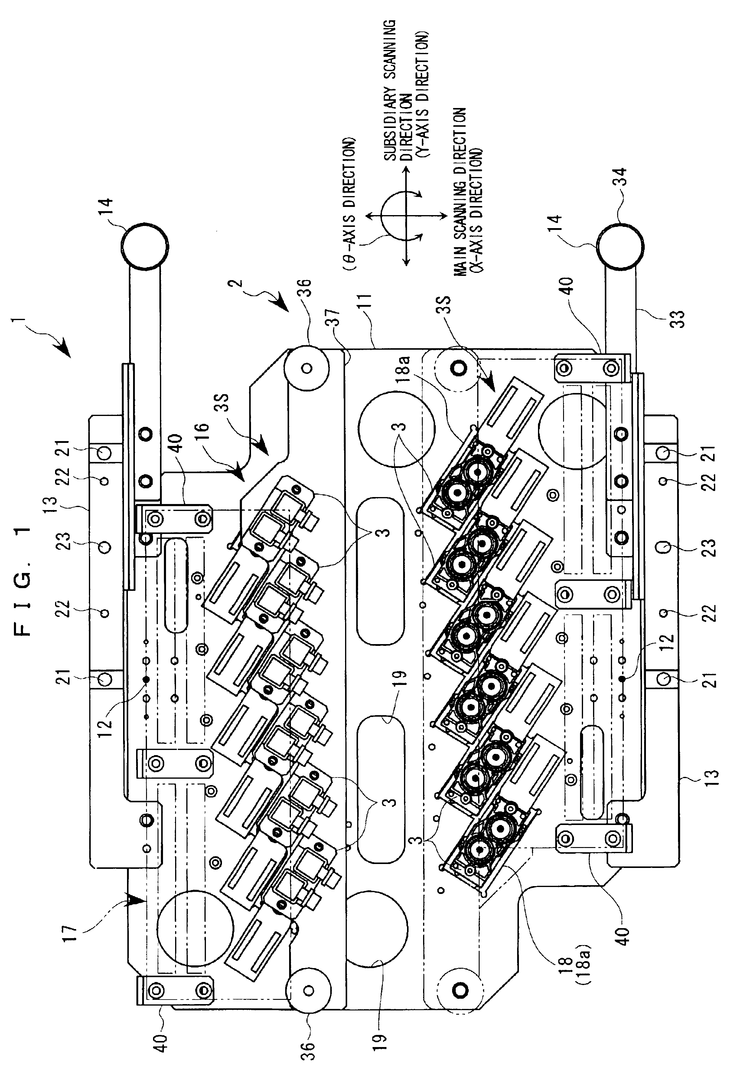
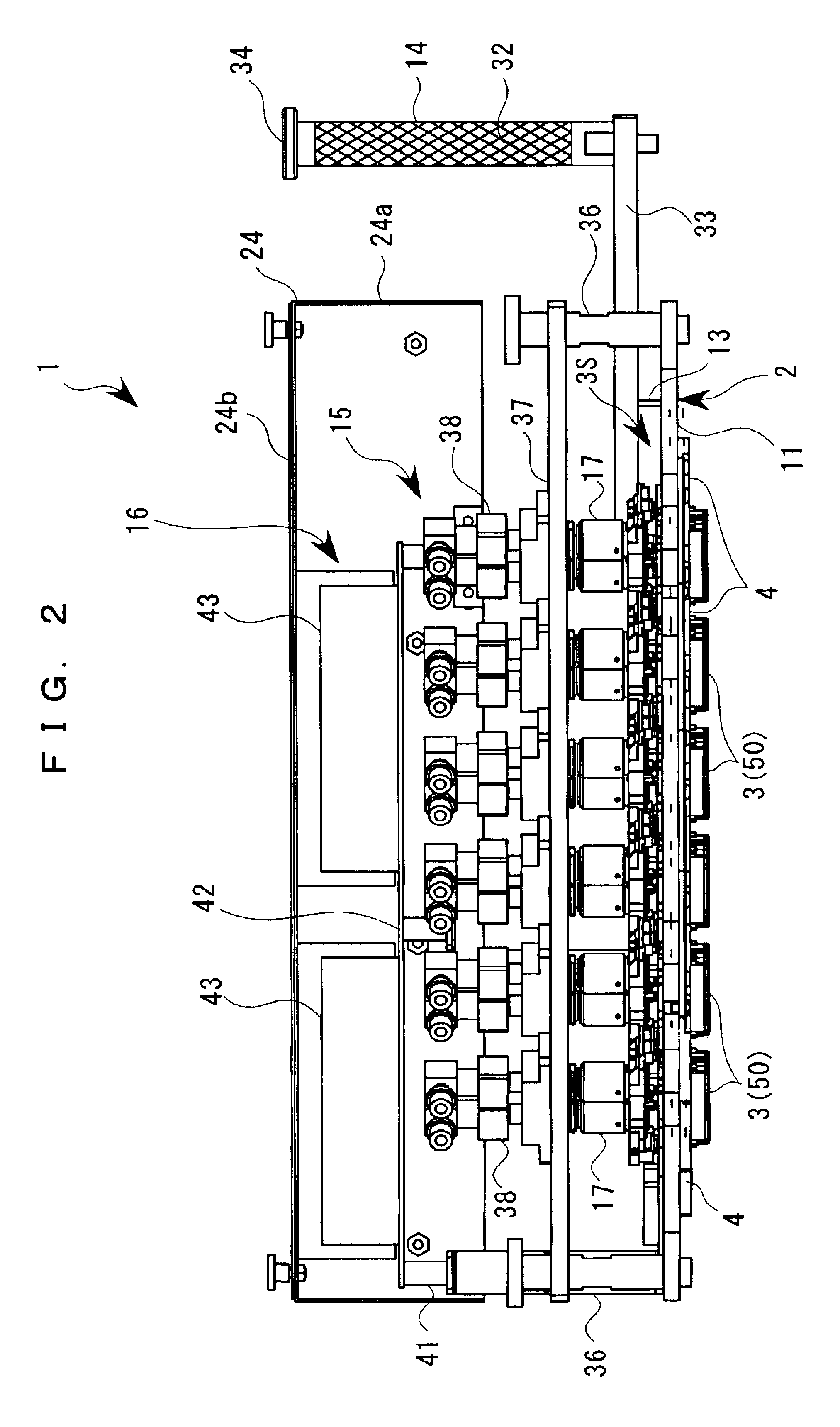
Member to be recognized for alignment; head unit and electronic device provided therewith; method of manufacturing lcd, organic el device, electron emission device, pdp device, electrophoretic display device, color filter, and organic el; method of forming spacer, metallic wire, lens, resist, and light diffusion member, each of said methods using said head unit
a technology of alignment and head unit, which is applied in the direction of electrophoretic display devices, electrode systems, instruments, etc., can solve the problems of affecting the alignment of the inability to secure the contrast between the corner portion of the carriage or the background, and the inability to recognize the alignmen
- Summary
- Abstract
- Description
- Claims
- Application Information
AI Technical Summary
Benefits of technology
Problems solved by technology
Method used
Image

Examples
first embodiment
(1) First Embodiment
[0276]FIGS. 54 through 58 show the first embodiment of this invention. In this embodiment, this invention is applied to the active matrix type of display device using EL display elements. In more concrete, there is shown an example in which a light emitting material as an optical material is coated by using scanning lines, signal lines, and common power supply lines as the wiring.
[0277]FIG. 54 is a circuit diagram showing part of the display device 600 in this embodiment. This display device 600 is made up of: a plurality of scanning lines 631; a plurality of signal lines 632 which extend in a direction crossing the scanning lines 631; and a plurality of common power supply lines 633 which extend in parallel with the signal lines 632, all disposed on a transparent substrate in a wired arrangement. At each of the crossing points between the scanning lines 631 and the signal lines 632, there are disposed pixel regions 600A.
[0278]The signal lines 632 are provided wi...
second embodiment
(2) Second Embodiment
[0308]FIGS. 60A and 60B show a second embodiment of this invention. This embodiment is one in which this invention is applied to a passive matrix type of display device using EL display elements.
[0309]FIG. 60A is a plan view showing the disposing relationship between a plurality of first bus wires 750 and a plurality of second bus wires 760 which are disposed at right angles thereto. FIG. 60B is a sectional view taken along the line B—B in FIG. 60A.
[0310]The same reference numerals are given to the same construction as that in the first embodiment, and the duplicated description is omitted. The detailed manufacturing steps are also the same as those of embodiment 1. Therefore, their illustration and description are omitted.
[0311]In this embodiment, an insulating film 770 of, e.g., SiO2, or the like, is disposed so as to enclose the predetermined position in which the light emitting element 641 is disposed. As a result, a level-difference portion 611 is formed be...
third embodiment
(3) Third Embodiment
[0313]FIG. 61 shows a third embodiment of this invention. In this embodiment, this invention is applied, in the same manner as in the first embodiment, to an active matrix type of display device using an EL display element. In particular, it is so arranged that a high accuracy patterning can be performed by forming the level-difference portion 611 utilizing the pixel electrode 642.
[0314]The same reference numerals are given to the same construction as above. FIG. 61 is a sectional view showing an intermediate state of the manufacturing step. Since the steps before and after the above are the same as those in embodiment 1, their illustration and description are omitted.
[0315]In this embodiment, the pixel electrode 642 is formed thicker than the ordinary one and the level-difference portion 611 is thereby formed. In other words, in this embodiment, there is formed a projected level-difference portion whose pixel electrode to which the optical material is coated aft...
PUM
 Abstract
Description
Claims
Application Information