CMOS image sensor having block scanning capability

a technology of image sensor and scanning capability, applied in the field of cmos image sensor, can solve the problems of large random noise, inability to read on a block-by-block basis, and inability to reset the photodiode, and achieve the effect of reducing random nois

Inactive Publication Date: 2005-08-23
KAWASAKI MICROELECTRONICS
View PDF20 Cites 32 Cited by
  • Summary
  • Abstract
  • Description
  • Claims
  • Application Information

AI Technical Summary

Benefits of technology

[0020]In view of the above-described problems of the known techniques, it is an object of the present invention to provide a CMOS image sensor that can output a signal containing reduced random noise in a block scanning fashion without needing either a block scanning circuit or a high-capacity frame memory for raster scanning.

Problems solved by technology

In an image system using an image sensor such as a CCD, raster scanning as shown in FIG. 1 is used because of the limitation associated with the device.
A problem of the former known technique described above is that reading cannot be performed on a block-to-block basis.
On the other hand, in the latter known technique described above, the photodiode cannot be reset, and thus there is large random noise.
Furthermore, because the signal voltage is not amplified in the pixel sensor 10 shown in FIG. 6, the signal is inevitably contaminated with 1 / f noise when being passed through three pass transistors, and also contaminated with coupling noise when being transmitted via a long interconnection line to the peripheral circuit.
Another problem is that color correction and motion detection are impossible, because only analog data subjected to two-dimensional DCT operation is available.

Method used


Image

  • CMOS image sensor having block scanning capability
  • CMOS image sensor having block scanning capability
  • CMOS image sensor having block scanning capability

Examples


Embodiment Construction

[0054]The present invention is described below in detail with reference to preferred embodiments in conjunction with the accompanying drawings.

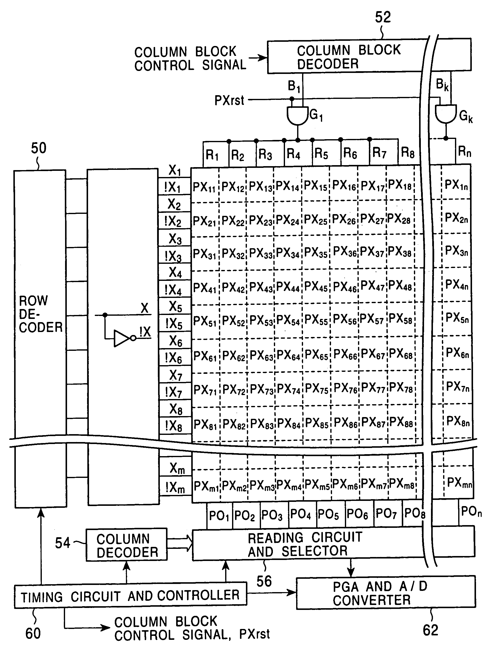
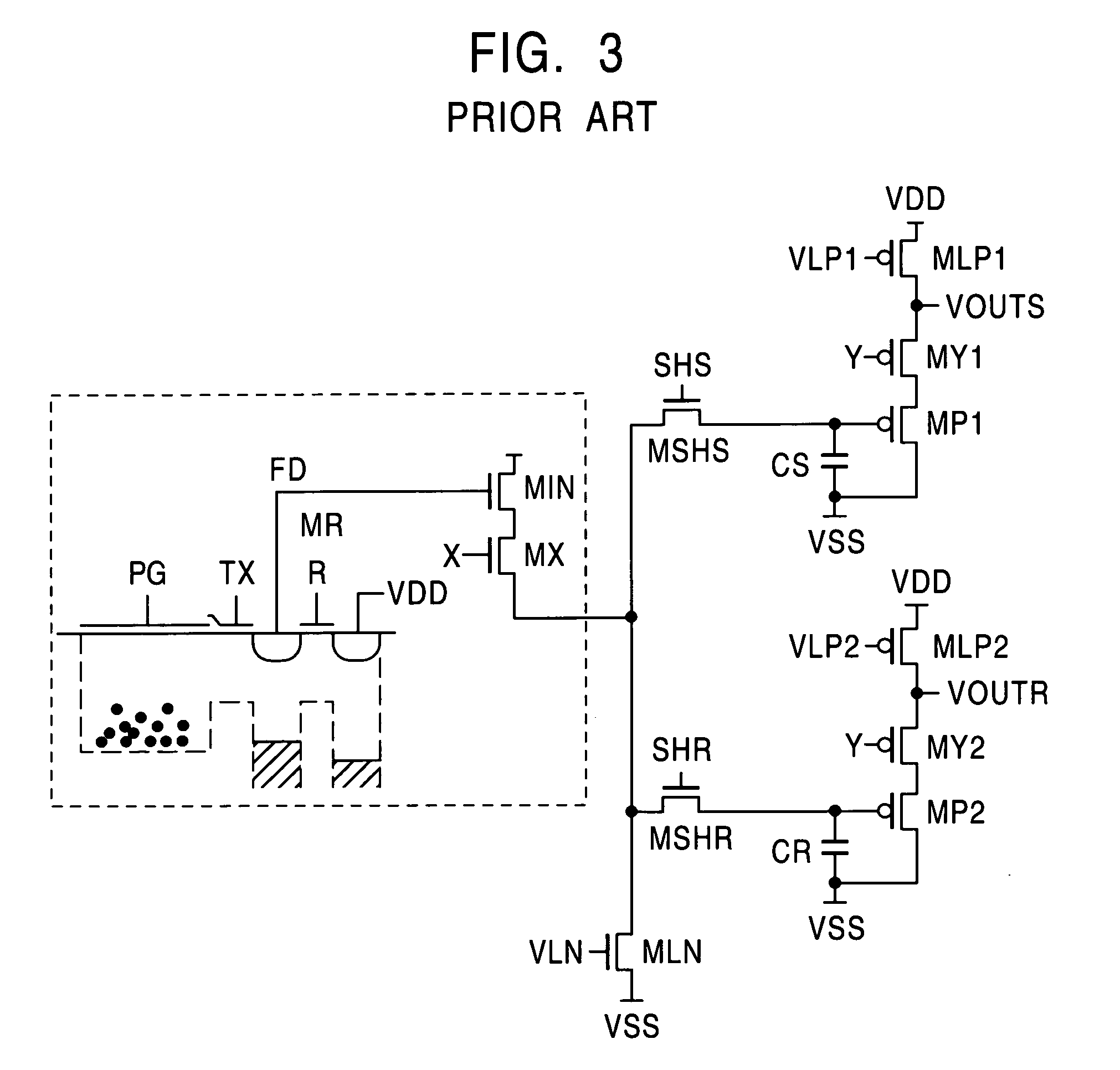
[0055]In circuit design and layout design for a pixel sensor, which is a unit of an area sensor, the following issues should be considered:[0056](1) The quantum efficiency should be sufficiently large. To this end, one important factor is a large aperture ratio.[0057](2) Random noise, which can cause a problem in particular in a CMOS image sensor, should be minimized.[0058](3) In order to fit a great number of pixel sensors in the form of an array, the size of each pixel sensor should be as small as possible.[0059](4) To minimize the size of the pixel sensor, each pixel sensor includes a single well and a single transistor.[0060](5) The number of elements, such as transistors, should be minimized.[0061](6) The number of interconnections to each pixel sensor should be minimized.[0062](7) An irregular arrangement of pixels causes spatial distor...


PUM


Abstract

A CMOS image sensor includes a plurality of pixel sensors arranged in a two-dimensional array. In each pixel sensor, a signal corresponding to the absolute value of the amount of incident light with reduced reset noise is obtained. The signals of the respective pixel sensors are then output in a block scanning fashion. The CMOS image sensor does not need to include a preprocessing circuit for discrete cosine transform or a high-capacity frame memory for raster scanning.

Description

BACKGROUND OF THE INVENTION[0001]1. Field of Invention[0002]The present invention relates to a CMOS image sensor, and, more particularly, to a CMOS image sensor that outputs data in a block scanning fashion, which can process without needing a preprocessing operation.[0003]2. Description of Related Art[0004]In an image system using an image sensor such as a CCD, raster scanning as shown in FIG. 1 is used because of the limitation associated with the device. When a still image is compressed according to the JPEG standard, which is a widely used standard, or when a moving image is compressed according to the MPEG standard, which is also widely used, Discrete Cosine Transform (DCT) is performed for a unit (block) including 8 pixels in a row by 8 pixels in a column. To this end, data associated with all pixels is first stored into a high-capacity frame memory, and then block-scanning is performed as shown in FIG. 2.[0005]CMOS image sensors are now receiving attention because of their ad...

Claims


Application Information

Patent Timeline
Patent Type & Authority Patents(United States)
IPC IPC(8): H01L27/146H04N5/335H04N5/217H04N5/341H04N5/345H04N5/357H04N5/363H04N5/369H04N5/374H04N5/378
CPCH04N3/155H04N3/1562H04N25/40H04N25/76H04N25/745
Inventor SAKO, NORIMITSU
Owner KAWASAKI MICROELECTRONICS
Why Eureka
Try Eureka