Jitter measurement circuit for measuring jitter of measurement target signal on the basis of sampling data string obtained by using ideal cyclic signal

a jitter measurement and target signal technology, applied in the direction of pulse characteristics measurement, instrumentation, transmission monitoring, etc., can solve the problems of disadvantageous cost, long construction time, and disadvantageous cost of testers having jitter measurement functions

Inactive Publication Date: 2005-08-23
RENESAS TECH CORP +1
View PDF26 Cites 27 Cited by
  • Summary
  • Abstract
  • Description
  • Claims
  • Application Information

AI Technical Summary

Benefits of technology

[0011]The foregoing and other objects, features, aspects and advantages of the present invention will become more appar...

Problems solved by technology

However, if a jitter measurement system is constructed with such measurement equipment or tester, it disadvantageously is expe...

Method used


Image

  • Jitter measurement circuit for measuring jitter of measurement target signal on the basis of sampling data string obtained by using ideal cyclic signal
  • Jitter measurement circuit for measuring jitter of measurement target signal on the basis of sampling data string obtained by using ideal cyclic signal
  • Jitter measurement circuit for measuring jitter of measurement target signal on the basis of sampling data string obtained by using ideal cyclic signal

Examples


first embodiment

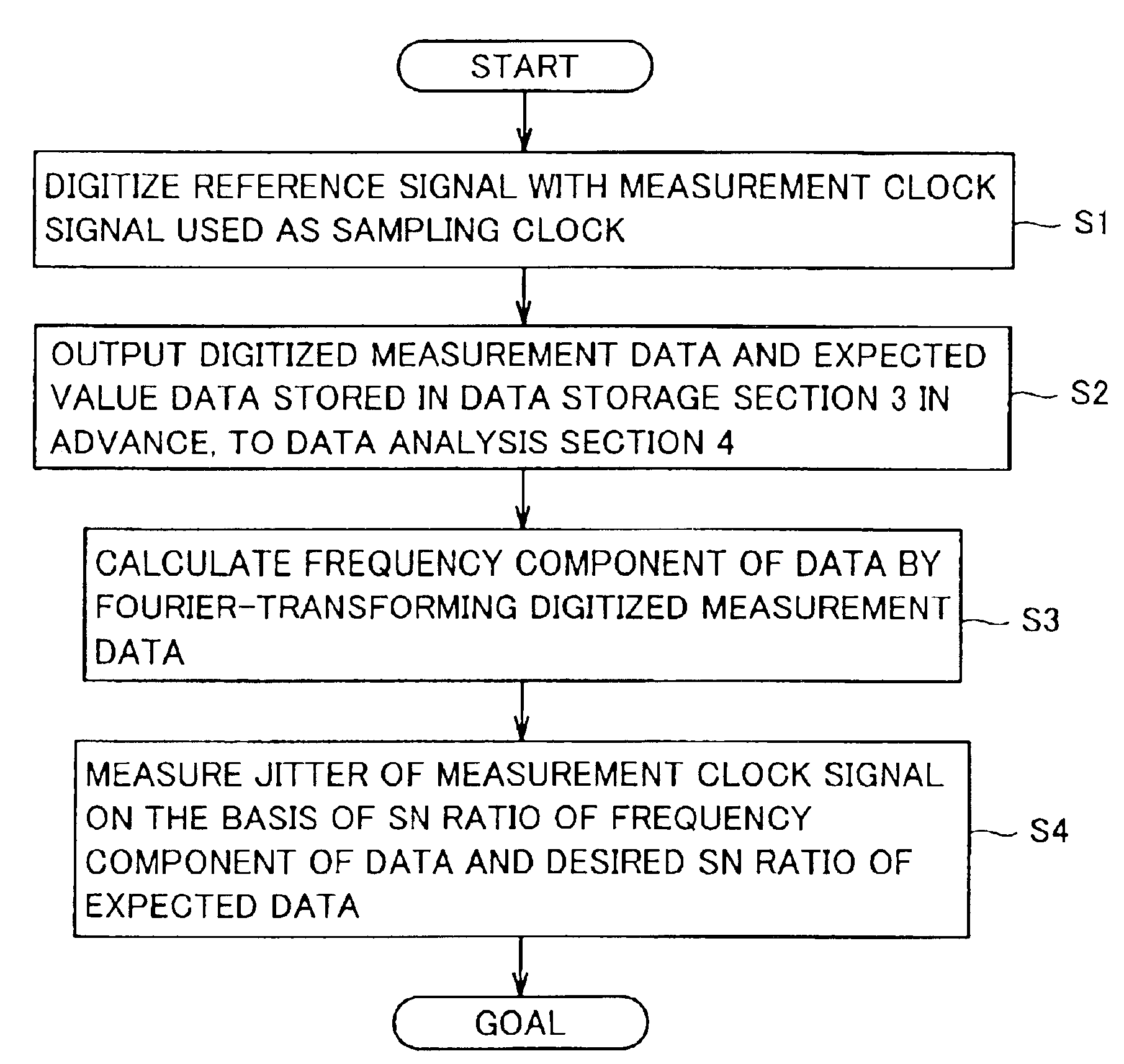
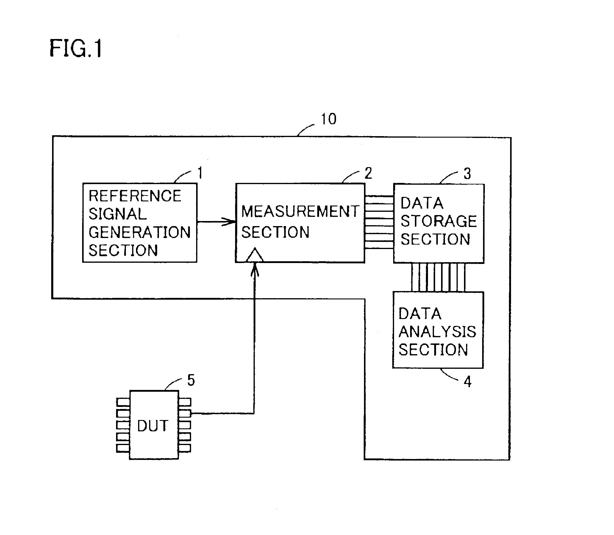
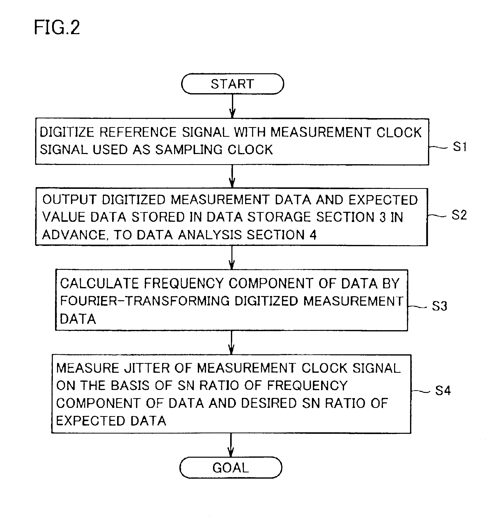
[0025]With reference to FIG. 1, a jitter measurement circuit 10 according to a first embodiment of the present invention includes: a reference signal generation section 1 which generates a high purity cyclic signal, that is, a constant and ideal cyclic signal; a measurement section 2 which analog-to-digital converts the amplitude of the signal outputted from reference signal generation section 1 with high accuracy; a data storage section 3 which stores data; and a data analysis section 4 which calculates a jitter quantity on the basis of the data stored in data storage section 3. An example of the cyclic signal generated by reference signal generation section 1 can includes a sine wave. Further, measurement section 2 receives an input with a measurement clock signal outputted from a measurement target DUT (Device Unit Testing) 5 using as a sampling clock.

[0026]Using the flow chart of FIG. 2, the operation of jitter measurement circuit 10 according to the first embodiment of the pres...

second embodiment

[0047]In the first embodiment, the constitution in which DUT 5 as a measurement target is directly measured by the jitter measurement circuit, has been described. In a second embodiment, the constitution of a semiconductor testing device which has functions according to the jitter measurement method shown in the first embodiment will be described.

[0048]With reference to FIG. 5, a semiconductor testing device 20 according to the second embodiment of the present invention includes: a control section 22 which controls overall semiconductor testing device 20; an internal bus 28 which transmits and receives data to and from an internal circuit; a test signal generation section 27 which executes the input / output of a test signal to and from measurement target DUT 5; and a jitter measurement section 30 which executes the measurement of the jitter of measurement target DUT 5.

[0049]Test signal generation section 27 is intended to input a test signal having a specific pattern into measurement...

first modification

of Second Embodiment

[0057]With reference to FIG. 6, a semiconductor testing device 21 according to a first modification of the second embodiment of the present invention differs from semiconductor testing device 20 shown in FIG. 5 in that jitter measurement section 30 is replaced by a jitter measurement section 31.

[0058]Since Jitter measurement section 31 is equal in constitution to jitter measurement circuit 11 according to the first modification of the first embodiment shown in FIG. 3, the connection relationship, the operation and the like of jitter measurement section 31 will not be repeatedly described herein. Thus, jitter measurement section 31 can execute the measurement of the jitter of the measurement clock signal outputted from DUT 5.

[0059]By including jitter measurement section 31 in the semiconductor testing device as seen in the constitution of the present invention, it is possible to attain the same advantages as those of the second embodiment described above.


PUM


Abstract

A jitter measurement circuit includes: a conversion section sampling one of a reference signal and a measurement target signal in response to the other of the signals, thereby obtaining a sampling data string; and a determination section measuring jitter of the measurement target signal on the basis of the sampling data string obtained by the conversion section. Since the reference signal is a stable signal having a predetermined cycle, the sampling data string as a measurement result depends on the measurement target signal. Therefore, it is possible to simply measure jitter level in accordance with irregularity of the measurement result and on the basis of relative measurement to expected value data.

Description

BACKGROUND OF THE INVENTION[0001]1. Field of the Invention[0002]The present invention relates to a jitter measurement circuit which measures jitter included in a cyclic signal.[0003]2. Description of the Background Art[0004]In recent years, there are seen the acceleration of the main clock bus of a personal computer, the emergence of high-rate interfaces such as IEEE-1394 interface, the rapid rising of digital radio transmission such as cellular phones or radio LAN including the Bluetooth and the like. Following them, the potential needs of the measurement of jitter are generally rising.[0005]There is known a jitter measurement method including quantizing a signal outputted from a measurement target object in the same cycle, and measuring the jitter of the signal in real time on the basis of the change of the quantized output data, as disclosed in Japanese Patent Laying-Open No. 2000-292469.[0006]Meanwhile, as equipment for measuring such jitter, a time interval analyzer which has a...

Claims


Application Information

Patent Timeline
IPC IPC(8): G01R29/26G01R29/00G01R29/02G01R31/28
CPCG01R29/26
Inventor HANAI, HISAYOSHIFUNAKURA, TERUHIKOMORI, HISAYA
Owner RENESAS TECH CORP
Why Eureka
Try Eureka