Inclusion of nitrogen at the silicon dioxide-silicon carbide interace for passivation of interface defects

a silicon dioxide and silicon carbide technology, applied in the direction of semiconductor devices, basic electric elements, electrical apparatus, etc., can solve the problems of low channel mobilities in sic mosfets, low quality of siosub>2/sub>/sic interface, and poorly understood oxidation kinetics and oxide interface of sic, so as to reduce the density of interface traps

Inactive Publication Date: 2005-09-06
VANDERBILT UNIV
View PDF7 Cites 34 Cited by
  • Summary
  • Abstract
  • Description
  • Claims
  • Application Information

AI Technical Summary

Benefits of technology

[0011]The present invention addresses this need by providing a method that reduces interface trap density in silicon carbide MOS devices and a semiconductor device with reduced interface trap density. This is accomplished by incorporating nitrogen at the SiO2 / SiC interface.

Problems solved by technology

However, the oxidation kinetics and oxide interface of SiC are poorly understood in comparison to Si.
Furthermore, the quality of the SiO2 / SiC interface is also inferior to the SiO2 / Si interface.
This problem causes low channel mobilities in SiC MOSFETS due to the density of interface states that exists in the band gap near the conduction band edge.
Initial studies of oxynitride films on 6H-SiC have shown a small improvement in MOS interface quality after NO anneal (reduction of the interface state and fixed charge densities takes place) but inferior MOS interface quality after N2O anneal.

Method used


Image

  • Inclusion of nitrogen at the silicon dioxide-silicon carbide interace for passivation of interface defects
  • Inclusion of nitrogen at the silicon dioxide-silicon carbide interace for passivation of interface defects
  • Inclusion of nitrogen at the silicon dioxide-silicon carbide interace for passivation of interface defects

Examples


example 1

Preparation of Annealed 4H-SiC Wafers

[0036]Preparation of silicon-faced (8° off axis) 4H-SiC wafers with a p-type substrate and epitaxial layer, doped at about 2×1016 cm−3 and n-type (100) Si wafers with a resistivity of about 10 Ω-cm required etching in a 10% HF solution to remove native oxide and thermal oxidation in a resistively heated quartz tube furnace. The 4H-SiC wafers were oxidized in wet oxygen (oxygen bubbled through deionized water at about 85-90° C. at a flow rate of about 1.0l / mm. The 4H-SiC wafers were then loaded in a wet oxidizing ambient at about 850° C., the temperature was raised to about 1150° C. and the samples were oxidized for about 30 minutes in accordance with prior art techniques. The ambient was then switched to argon, the temperature was lowered to about 800° C. and the SiC wafers were removed from the furnace. The oxide thickness for the SiC wafers was about 30 nm.

[0037]When annealing was carried out with 15N containing gases the following conditions w...

example 2

Preparation of Annealed 4H-Si Wafers

[0039]Si wafers were oxidized in dry oxygen (2O) at a flow rate of about 1 l / min, loaded in a oxidizing ambient at about 900° C. and oxidized at about 900° C. for about 25 minutes. The ambient was then switched to argon, and the Si wafers were removed from the furnace. The oxide thickness for Si wafers was about 20 nm.

[0040]The Si wafers were then annealed in a resistively heated quartz tube furnace with 99.7% 15N18O or 15N2O at a static pressure of about 10 mbar at about 1000° C. for either about 1 or about 4 hours. When annealing was carried out with 14N containing gases the conditions specified above were typically used. Anneals were preferably carried out at gas flow rates of about 0.5 l / min at atmospheric pressure, at temperatures between about 1000° C. and about 1200° C. for between about one and about six hours.

example 3

Measurement of Areal Densities

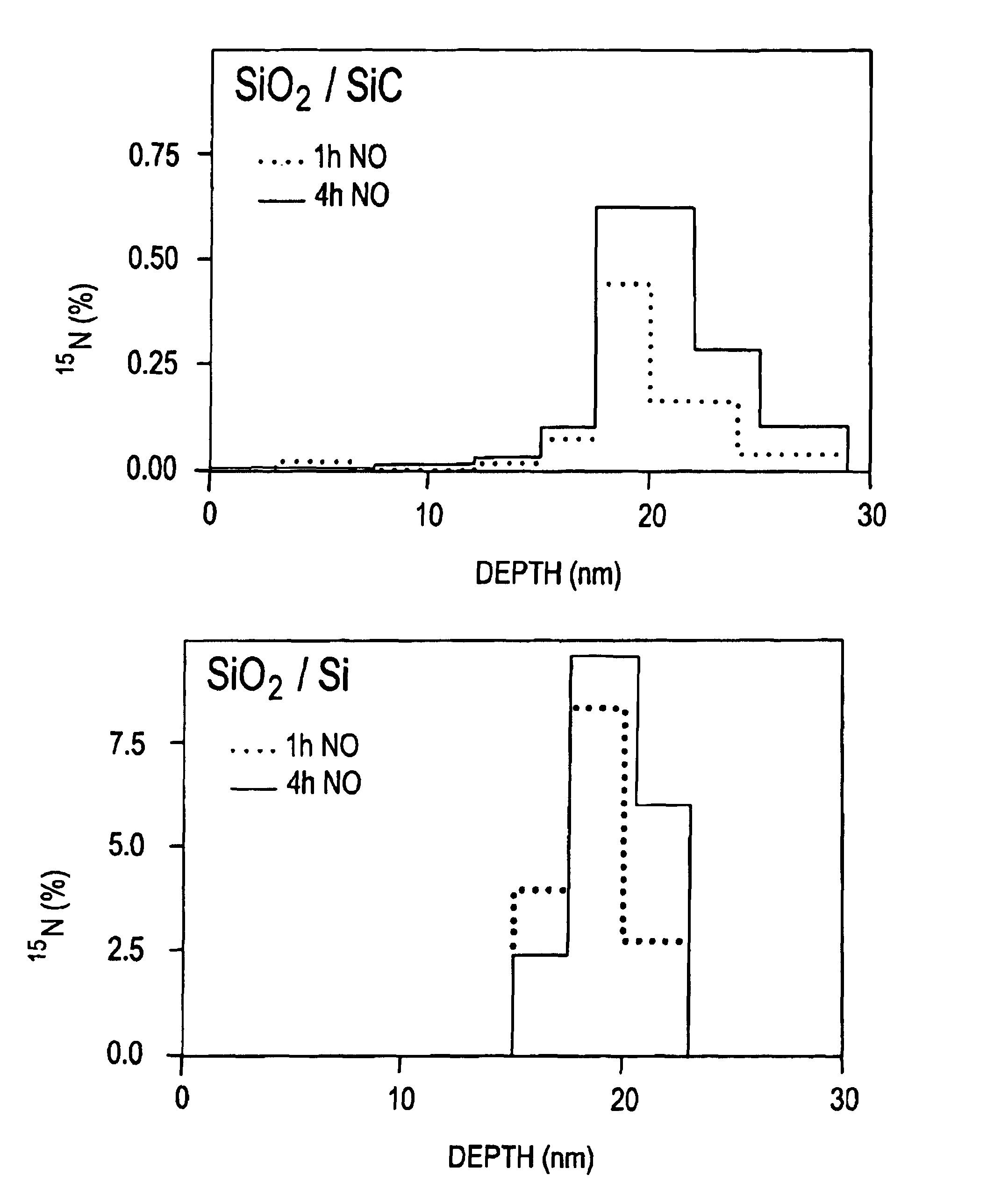
[0041]The areal densities of 15N and 18O of annealed Si / C and Si wafers prepared as described in Examples 1 and 2 were determined by Nuclear Reaction Analysis (NRA) using the reactions 15N(p,αγ) 12C at Ep=1 MeV and 18O(p,αγ)15N at Ep=730 keV. The 15N and 18O depth profiles were determined by nuclear resonance profiling (NRP) using the resonances in the reactions 15N(p,αγ)12C at 429 keV and 18O(p,α)15N at 151 keV, respectively, and a tilted sample geometry (ψ=65°). The measured excitation curves (γ or a yield versus incident proton energy) around the resonance energy were converted into concentration versus depth profiles. Table 1, shown below summarizes oxidation conditions, anneal times, oxide thickness and areal densities for a number of experiments.

[0042]

TABLE 115N 18OAnneal15N Areal18O ArealOxideOxidationTimeDensityDensityThicknessMaterialConditions(hours)(1015 cm−2)(1015 cm−2)(nm)Si900° C.-Dry11.619.620.3Si900° C.-Dry42.244.622.8SiC1150° C.-10.115....


PUM

PropertyMeasurementUnit
temperatureaaaaaaaaaa
thicknessaaaaaaaaaa

Abstract

A method for manufacturing a silicon carbide semiconductor device. In one embodiment, the method includes the following steps: a layer of silicon dioxide is formed on a silicon carbide substrate to create a silicon dioxide/silicon carbide interface and then nitrogen is incorporated at the silicon dioxide/silicon carbide interface for reduction in an interface trap density. The silicon carbide substrate, in one embodiment, includes a n-type 4H-silicon carbide.

Description

[0001]This application claims the benefit under 35 U.S.C. §119(e) of U.S. Provisional Application No. 60 / 192,009, filed Mar. 24, 2000, which is incorporated herein by reference in its entirety.STATEMENT REGARDING FEDERALLY SPONSORED RESEARCH OR DEVELOPMENT[0002]This invention was made with government support under grant #MDA972 98-1-0007 awarded by the Defense Advanced Research Projects Agency (DARPA). The federal government has certain rights in the present invention.BACKGROUND OF THE INVENTION[0003]1. Field of the Invention[0004]The present invention relates to silicon carbide semiconductor devices and methods for their construction. More specifically, the instant invention relates to silicon carbide semiconductor devices with a layer of silicon dioxide disposed on a silicon carbide substrate that have a region of substantial nitrogen concentration at the silicon dioxide-silicon carbide interface.[0005]2. Description of the Related Art[0006]Presently, the silicon (Si) metal-oxide-...

Claims


Application Information

Patent Timeline
Patent Type & Authority Patents(United States)
IPC IPC(8): H01L21/02H01L21/3115H01L21/04
CPCH01L21/0214H01L21/02164H01L21/02236H01L21/02238H01L21/02255H01L21/02332H01L21/02337H01L21/045H01L21/049H01L21/3145H01L21/31658H01L29/513H01L29/518H01L29/66068H01L29/1608Y10S438/931
Inventor CHUNG, GILYONGTIN, CHIN CHEWILLIAMS, JOHN R.MCDONALD, KYLEVENTRA, MASSIMILIANO DIWELLER, ROBERT A.PANTELIDES, SOKRATES T.FELDMAN, LEONARD C.
Owner VANDERBILT UNIV
Why Eureka
Try Eureka