Analog to digital converter with a pulse delay circuit

a technology of delay circuit and analog to digital converter, which is applied in the field of analogtodigital converter, can solve the problems of increasing and achieve the effect of reducing the power consumption of a/d converter

Active Publication Date: 2005-09-06
DENSO CORP
View PDF15 Cites 27 Cited by
  • Summary
  • Abstract
  • Description
  • Claims
  • Application Information

AI Technical Summary

Benefits of technology

[0015]The present invention is made on the background so that preferable embodiments of the present invention can reduce power consumption of an A / D converter with a pulse delay circuit.

Problems solved by technology

This tunneling current Ya may cause power consumption of the A / D converter to increase.

Method used


Image

  • Analog to digital converter with a pulse delay circuit
  • Analog to digital converter with a pulse delay circuit
  • Analog to digital converter with a pulse delay circuit

Examples


first embodiment

[First Embodiment]

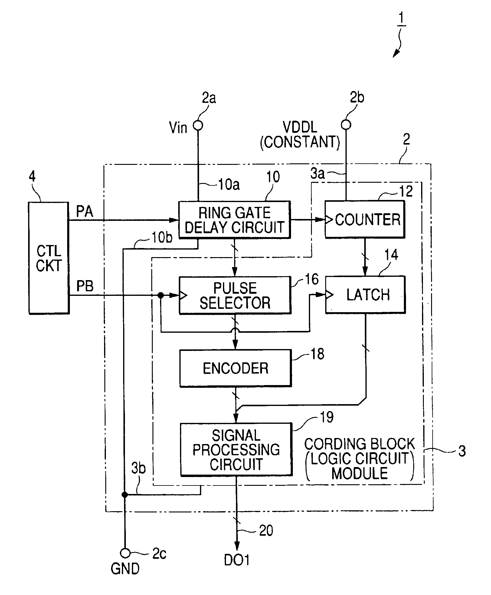
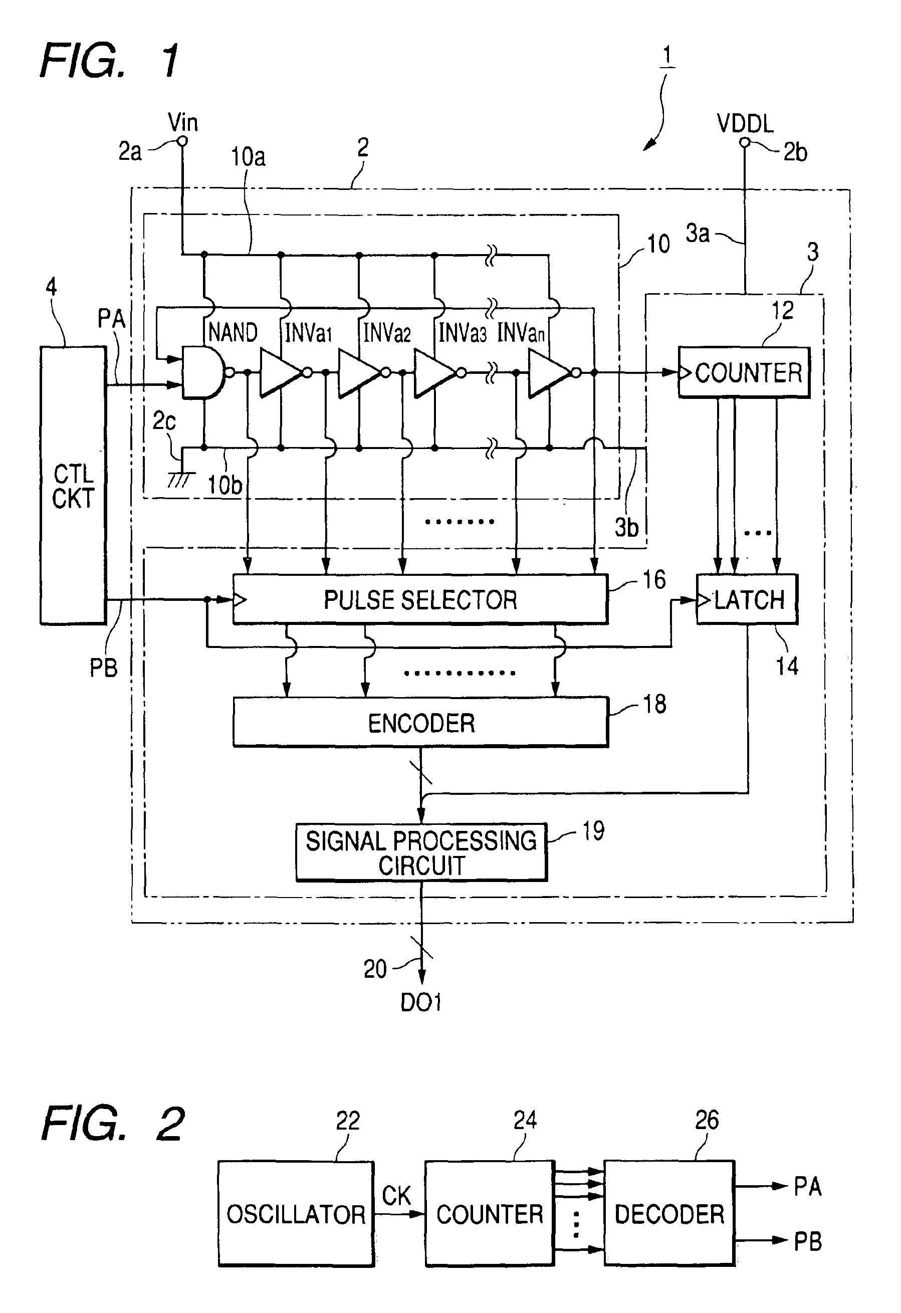
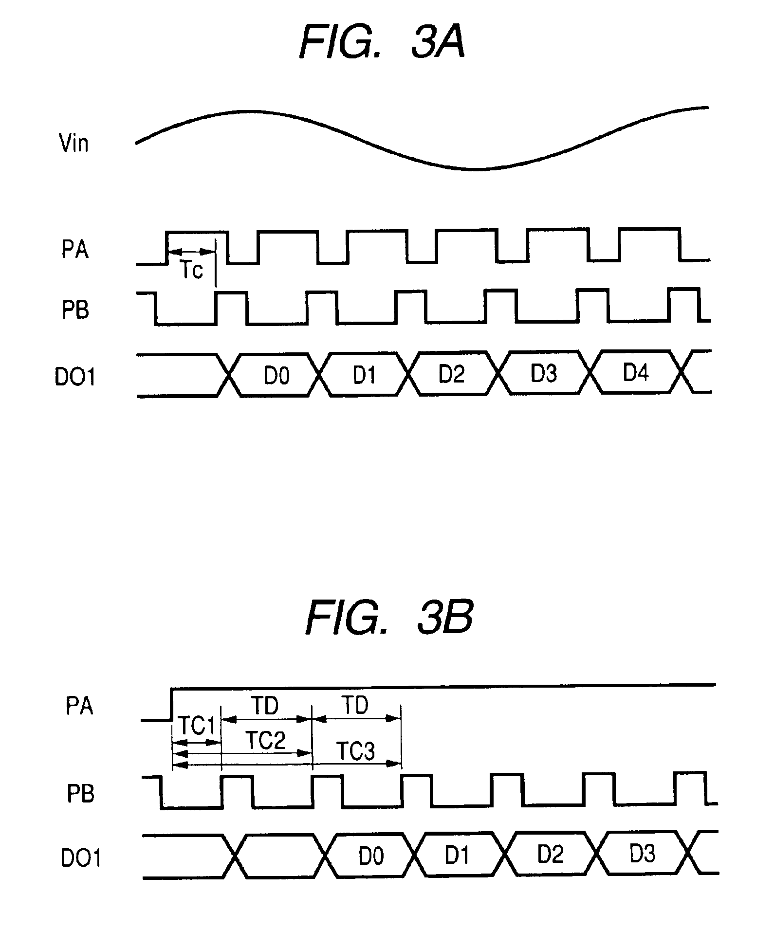
[0036]As shown in FIG. 1, an A / D converter 1 according to a first embodiment of the present invention is provided with a control circuit 4 for generating pulse signals PA and PB. The A / D converter 1 is provided with a pulse phase difference coding circuit 2 having one and other input terminals 2a and 2b for coding a phase difference between the pulse signals PA and PB.

[0037]The pulse phase difference coding circuit 2 is provided with a ring-gate delay circuit 10. The ring-gate delay circuit 10 is preferably composed of an odd number (for example, 15) of inverting circuits. Specifically, as the odd number of inverting circuits, a NAND gate NAND and an even number of inverters INVa1 to INVan (n: even number) are preferably used. The NAND gate NAND has one and other input terminals and one output terminal, and is designed so that the pulse signal PA is inputted to the one input terminal thereof.

[0038]In particular, the NAND gate NAND and the inverters INVa1 to INVan a...

second embodiment

[Second Embodiment]

[0094]An A / D converter according to a second embodiment of the present invention has the substantially same structure as the structure of the A / D converter 1 of the first embodiment except for the set of the input voltage range of the voltage signal Vin and the power supply voltage VDDL. Elements of the A / D converter according to the second embodiment are assigned to the same reference characters as the A / D converter 1 shown in FIG. 1 and so on.

[0095]In the A / D converter according to the second embodiment, the power supply voltage VDDL is set to a range equal to or higher than the Vmax (=|Vthn|+|Vthp|), and the input voltage range of the voltage signal Vin and the power supply voltage VDDL is set to meet the relationship represented by the following equation:

VDDL−|Vthp|≦Vin≦VDDL

[0096]This relationship of the voltage signal Vin and the power supply voltage VDDL allows the p-channel transistor 40pT and the n-channel transistor 40nT of at least one of the logic gates...


PUM


Abstract

An A / D converter has a pulse delay circuit including a plurality of inverting circuits to each of which an analog voltage signal is inputted through a first pair of power supply lines. Each of the inverting circuits has a first logic gate. The A / D converter has a logic circuit having a second logic gate and a second pair of power supply lines, the logic circuit operating based on a power supply voltage. At least one of a first range of a level of the voltage signal and a second range of the power supply voltage is set to prevent a tunneling current from flowing at least one of between the first paired power supply lines and between the second paired power supply lines when at least one of first and second logic gates operates.

Description

CROSS REFERENCE TO RELATED APPLICATION[0001]This application is based upon and claims the benefit of priority of the prior Japanese Patent Application 2003-324823 filed on Sep. 17, 2003 so that the descriptions of which are incorporated herein by reference.BACKGROUND OF THE INVENTION[0002]1. Field of the Invention[0003]The present invention relates to an analog-to-digital converter for converting an analog signal to digital data, which is referred to simply as “A / D converter” hereinafter. In particular, the present invention relates to an A / D converter having a pulse delay circuit for sending a pulse signal while delaying the pulse signal in stages.[0004]2. Description of the Related Art[0005]A / D converters each including a pulse delay circuit having inverters connected in series and adapted to send a pulse signal while delaying it in stages have been well known. In particular, A / D converters each including a ring-gate delay circuit, as one type of the pulse delay circuit have also ...

Claims


Application Information

Patent Timeline
Patent Type & Authority Patents(United States)
IPC IPC(8): H03M1/00H03M1/50H03M1/64H03M1/06H03M1/14
CPCG04F10/005H03M1/06H03M1/14H03M1/502H03M1/60
Inventor TERAZAWA, TOMOHITOWATANABE, TAKAMOTO
Owner DENSO CORP
Why Eureka
Try Eureka