Method of etching magnetic and ferroelectric materials using a pulsed bias source

a magnetic and ferroelectric material and bias source technology, applied in the direction of nanoinformatics, chemistry apparatus and processes, cleaning using liquids, etc., can solve the problems of low efficiency and productivity of such processes, electrical short circuits within mram or feram devices, and difficult to remove conductive post-etch residues on the film stack, etc., to reduce plasma-related damage and eliminate the formation of conductive residues

Inactive Publication Date: 2005-09-13
APPLIED MATERIALS INC
View PDF40 Cites 17 Cited by
  • Summary
  • Abstract
  • Description
  • Claims
  • Application Information

AI Technical Summary

Benefits of technology

[0011]In exemplary applications, the method is used for fabricating magneto-resistive random access memory (MRAM) and ferroelectric random access memory (FeRAM) devices to eliminate formation of conductive residues upon film stacks of the devices and to reduce plasma-related damage.

Problems solved by technology

During etching of these materials, the materials may leave difficult to remove conductive post-etch residues upon the film stack.
The conductive residues or eroded layers may cause electrical short-circuits within the MRAM or FeRAM device.
The disadvantage of the wet cleaning processes are low efficiency and productivity of such processes, lack of real time (i.e., in situ) end point detection, as well as a need in dedicated equipment that may be incompatible with vacuumed plasma etch reactors used during fabrication of the MRAM device.

Method used


Image

  • Method of etching magnetic and ferroelectric materials using a pulsed bias source
  • Method of etching magnetic and ferroelectric materials using a pulsed bias source
  • Method of etching magnetic and ferroelectric materials using a pulsed bias source

Examples


Embodiment Construction

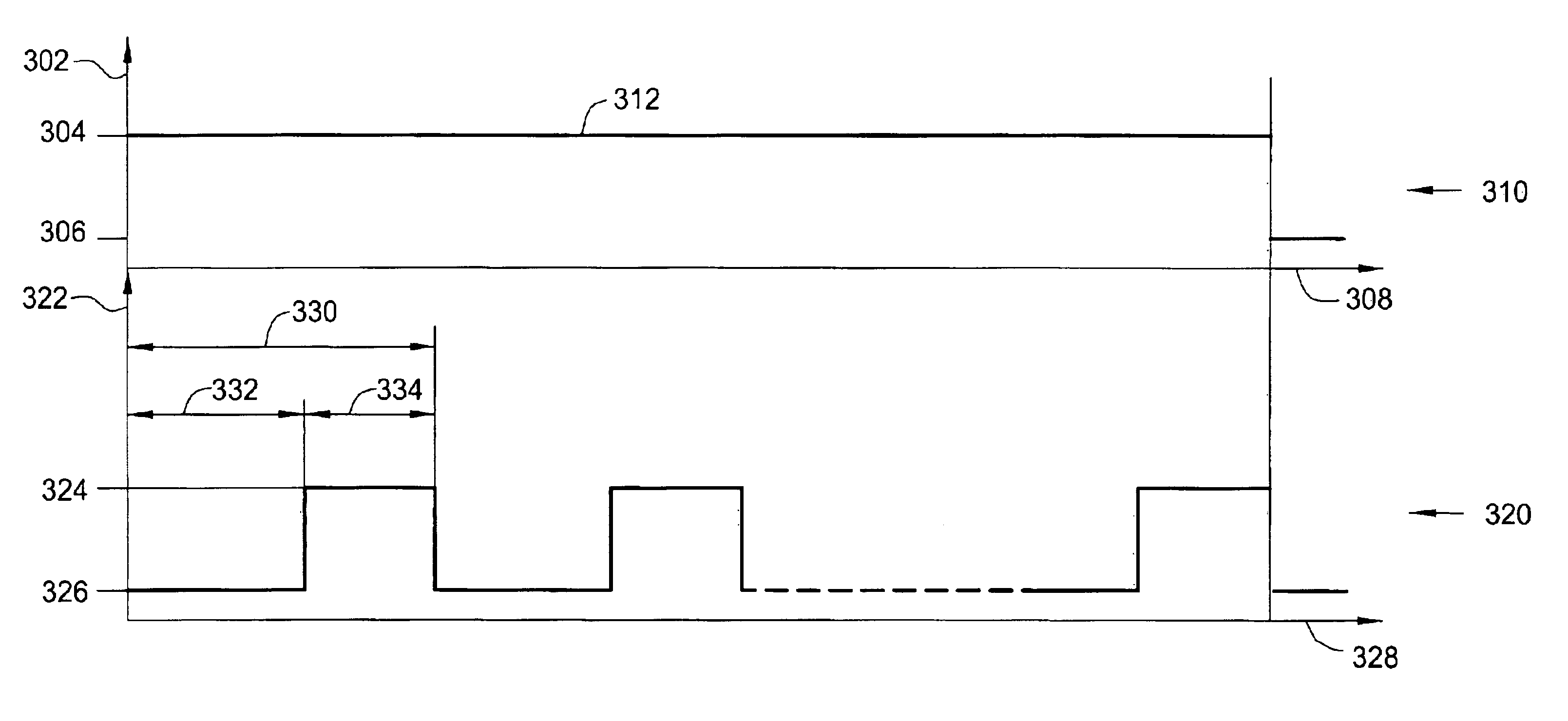
[0021]The present invention is a method for etching magnetic and ferroelectric materials on a semiconductor substrate. The method uses a pulsed substrate biasing technique (PSBT) that applies a plurality of processing cycles to the substrate, where each cycle comprises a period of plasma etching without substrate bias and a period of plasma etching with the substrate bias.

[0022]In exemplary applications, the method is used for fabricating magneto-resistive random access memory (MRAM) devices and ferroelectric random access memory (FeRAM) devices to eliminate formation of conductive post-etch residues upon the film stacks of the devices and to reduce plasma-related damage.

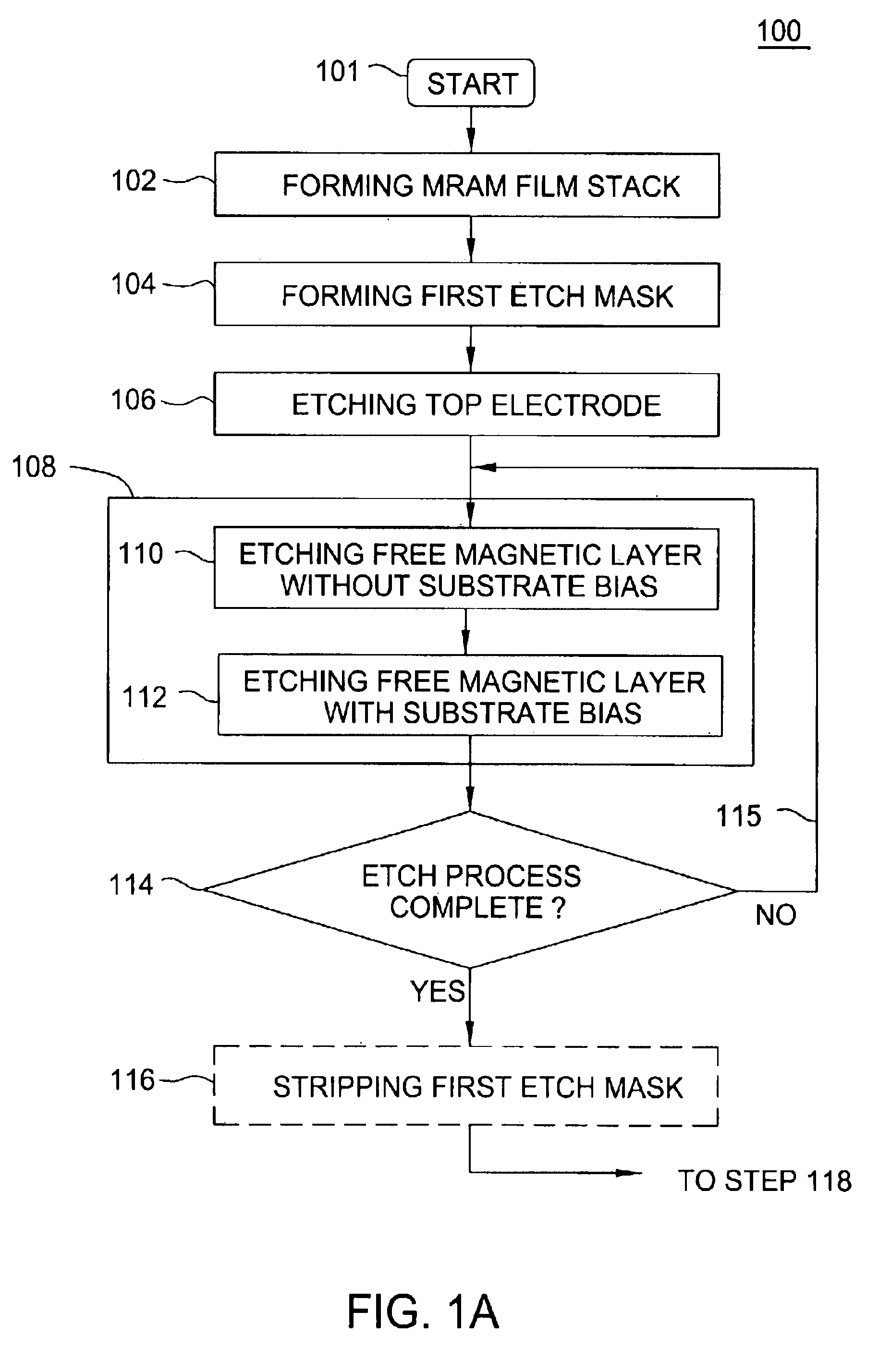
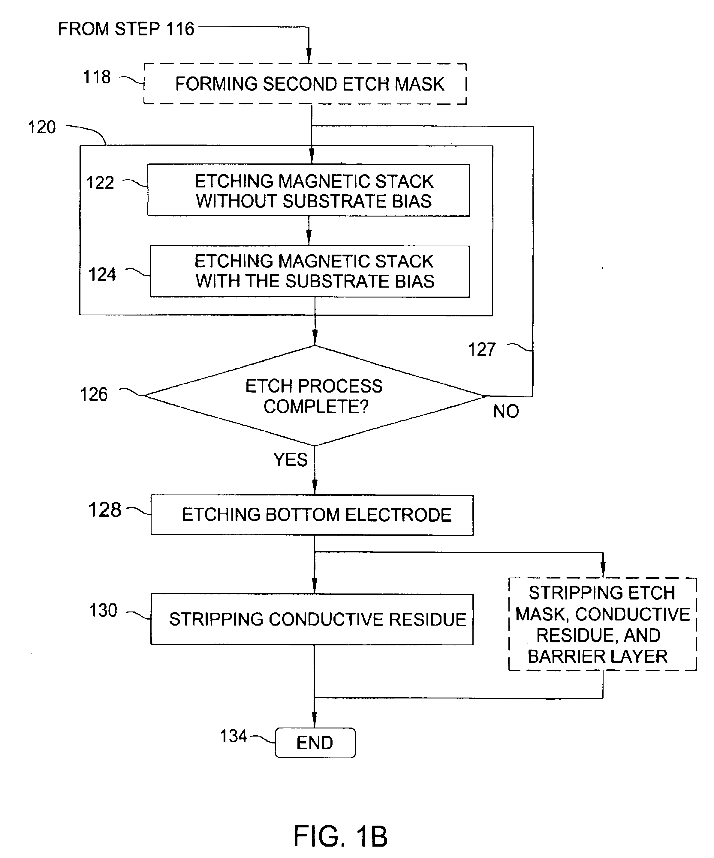
[0023]FIGS. 1A-1B depicts a flow diagram of a method 100 of fabricating a MRAM device in accordance with the present invention. The method 100 comprises processes that are performed upon a MRAM film stack during fabrication of the MRAM device.

[0024]FIGS. 2A-2L, together, depict a sequence of schematic, cross-section...


PUM

PropertyMeasurementUnit
pressureaaaaaaaaaa
poweraaaaaaaaaa
poweraaaaaaaaaa

Abstract

A method for etching magnetic and ferroelectric materials using a pulsed substrate biasing technique (PSBT) that applies a plurality of processing cycles to the substrate, where each cycle comprises a period of plasma etching without substrate bias and a period of plasma etching with the substrate bias. In exemplary applications, the method is used for fabricating magneto-resistive random access memory (MRAM) and ferroelectric random access memory (FeRAM) devices.

Description

BACKGROUND OF THE INVENTION[0001]1. Field of the Invention[0002]The present invention generally relates to a method for fabricating devices on semiconductor substrates. More specifically, the present invention relates to a method of etching magnetic and ferroelectric materials.[0003]2. Description of the Related Art[0004]Microelectronic devices are generally fabricated on a semiconductor substrate as integrated circuits wherein various conductive layers are interconnected to one another to facilitate propagation of electronic signals within the device. An example of such a device is a storage element in magneto-resistive random access memories (MRAM) or ferroelectric random access memories (FeRAM).[0005]MRAM and FeRAM comprise a plurality of memory cells that are interconnected to one another to facilitate storage of digital information. In MRAM, digital information is stored in a form of the direction of magnetization of a magnetic material, and in FeRAM the information is stored i...

Claims


Application Information

Patent Timeline
Patent Type & Authority Patents(United States)
IPC IPC(8): C23F4/00H01F41/30H01F41/14H01L21/70H01L21/8246H01L21/02H01L21/3213H01L21/311
CPCB82Y10/00B82Y25/00B82Y40/00C23F4/00H01F41/301H01F41/308H01L43/12H01J2237/3348H01L21/31122H01L21/32136H01L27/228H10B61/22H10N50/01
Inventor YING, CHENTSAUNALLAN, PADMAPANI C.KUMARCHEN, XIAOYI
Owner APPLIED MATERIALS INC
Why Eureka
Try Eureka