

Semiconductor device and manufacturing method for same
- Summary
- Abstract
- Description
- Claims
- Application Information
AI Technical Summary
Benefits of technology
Problems solved by technology
Method used
Image

Examples
embodiment 1
[Embodiment 1]
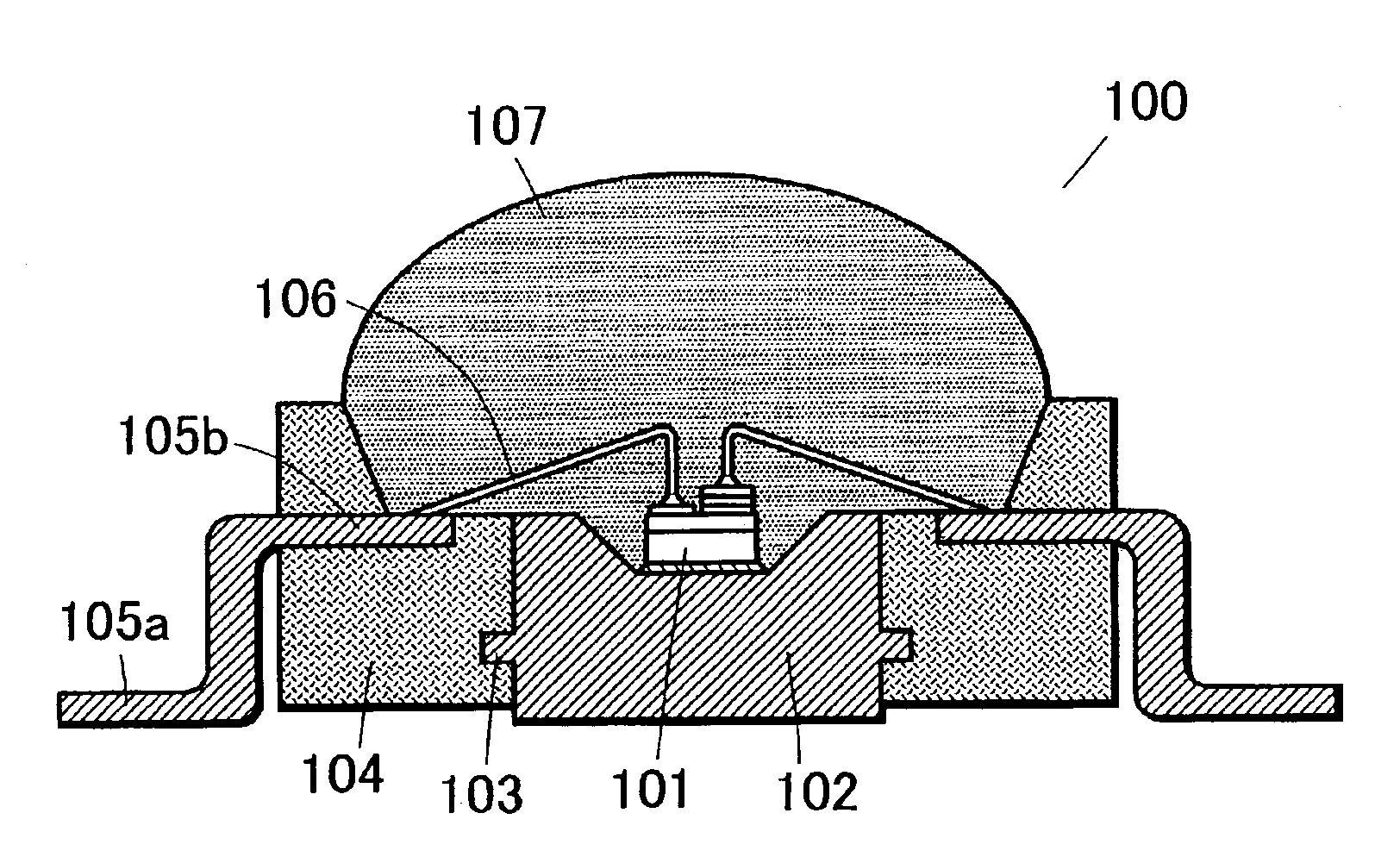
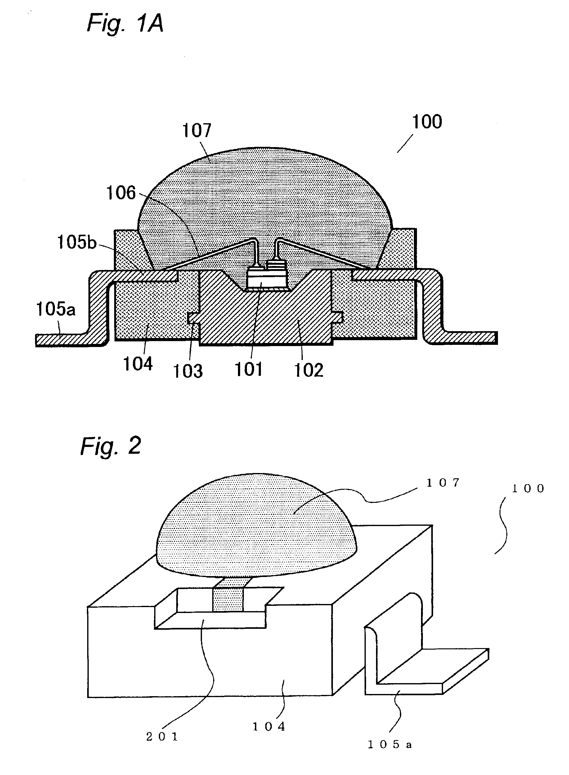
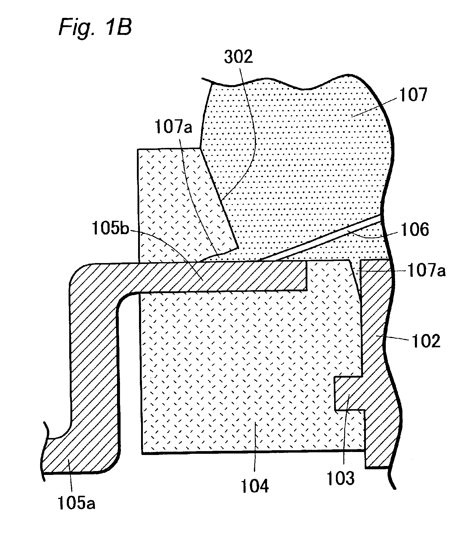
[0095]As shown in FIG. 3, package support part 104 utilized in the formation process of the present embodiment is formed at the center of frame 300 of a thermoplastic resin according to an injection molding process so that the upper surface of injection frame 305, through which the resin passes at the time of injection of the mold material, and the main surface of package 104 (surface existing at the highest level from among surfaces on the side in which recess 302 is created, except for the surface formed of notches 201, recess 302 and gates 306) are included in the same plane. In addition, notches 201 provided in the upper portion of package support part 104 are recesses having dimension approximately equal to the dimensions of the tips of the lead frames (air vent frame 303 and injection frame 305) and the tips of the lead frames are placed so as to make close contact with, and so as to be caught by, notches 201. Accordingly, the tips can easily be removed from notc...
embodiment 2
[Embodiment 2]
[0109]A semiconductor device is formed in the same manner as in Embodiment 1 except for the utilization of a variety of thermoplastic resins having softening points in the range of 85° C. to 120° C. as the thermoplastic material.
[0110]By doing the above, the occurrence of resin burrs can be prevented, the task efficiency can be increased so that a semiconductor device of a high reliability can be formed.
embodiment 3
[Embodiment 3]
[0111]FIG. 5 is a schematic top view showing the state of a light emitting device according to the present Embodiment 3 after an LED chip has been provided in a containment part of the package and wiring has been carried out before mold member 107 is formed, wherein the configuration of the bonding parts differs from that of Embodiment 1.
[0112]Here, the main surface of the heat sink is exposed from the bottom of the recess in the package according to the present Embodiment 3 in the same manner as in Embodiment 1 and LED chip 101 is provided in the recess created in the main surface of this exposed heat sink wherein, as shown in FIG. 5, the positive electrode and the negative electrode of this LED chip 101 are connected to the lead electrodes.
[0113]Here, in the present Embodiment 3, the positive electrode and the negative electrode, respectively, of LED chip 101 have a plurality of bonding parts and each of these pluralities of bonding parts is wire bonded to an inner l...
PUM
| Property | Measurement | Unit |
|---|---|---|
| Area | aaaaa | aaaaa |
| Fluorescence | aaaaa | aaaaa |
| Thermoplasticity | aaaaa | aaaaa |
Abstract
Description
Claims
Application Information