Compensation mechanism for compensating bias levels of an operation circuit in response to supply voltage changes

a technology of bias level and operation circuit, which is applied in the field of analog circuits, can solve the problems of increasing the dynamic range of the amplifier powered by the battery, the voltage provided by the battery tends to degrade, and the amplifier may no longer operate in the linear range, so as to increase the resistance, decrease the bias level, and increase the resistance

Inactive Publication Date: 2005-09-13
HONEYWELL INC
View PDF5 Cites 10 Cited by
  • Summary
  • Abstract
  • Description
  • Claims
  • Application Information

AI Technical Summary

Benefits of technology

[0025]In use, if the voltage at the drain (or source) of the differential pair of transistors is higher than a predetermined reference voltage, the comparator increases the voltage at the gate terminals of the bypass transistors. This increases the resistance between the source of the differential pair of transistors and the supply voltage, and for a given source / drain current, decreases the bias level at the drain (or source) of the differential pair of transistors. Likewise, if the voltage at the drain (or source) of the differential pair of transistors is lower than the reference voltage, the comparator decreases the voltage at the gate of the bypass transistors. This decreases the resistance between the source of the differential pair of transistors and the supply voltage, and for a given source / drain current, increases the bias level at the drain (or source) of the differential pair of transistors. What is provided, then, is a compensation circuit that can dynamically compensate selected bias levels within an operational circuit (e.g., amplifier) to maintain operation and performance over a relatively wide range of supply voltages.

Problems solved by technology

If critical amplifying devices enter saturation, the amplifier may no longer operate in the linear range.
The minimum usable input signal is often dictated by the internal noise of the amplifier.
As is known, however, the voltage provided by batteries tends to degrade over time, especially for alkaline batteries.
Accordingly, the dynamic range of an amplifier that is powered by a battery will tend to degrade over time.
Moreover, if the supply voltage degrades beyond some critical point, some or all of the amplifying devices may enter saturation and the amplifier may cease to operate in a linear mode.
A limitation of this approach is, of course, that the performance of the amplifier is typically less than optimal under nominal conditions.
Further, the design constraints imposed by designing an amplifier that uses fixed bias levels to maintain satisfactory performance over all operating conditions can increase the complexity of the design.

Method used


Image

  • Compensation mechanism for compensating bias levels of an operation circuit in response to supply voltage changes
  • Compensation mechanism for compensating bias levels of an operation circuit in response to supply voltage changes
  • Compensation mechanism for compensating bias levels of an operation circuit in response to supply voltage changes

Examples


Embodiment Construction

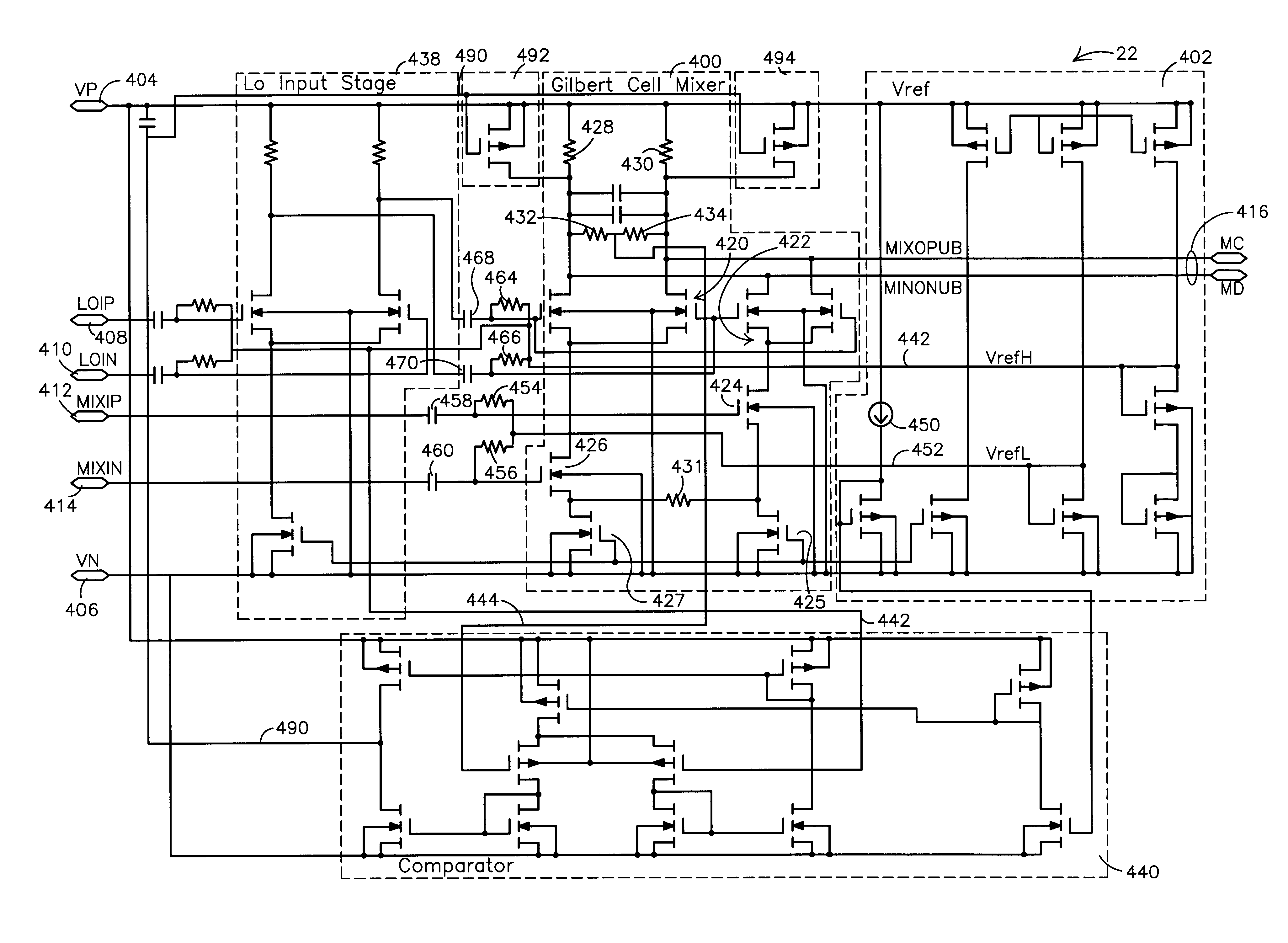
[0032]The present invention provides a compensation circuit that can dynamically compensate bias levels of selected devices of an operational circuit (e.g., amplifier) in response to variations in the supply voltage. The compensation circuit changes the bias levels in view of variations in the supply voltage so that functionality and performance of the operational circuit are substantially maintained.

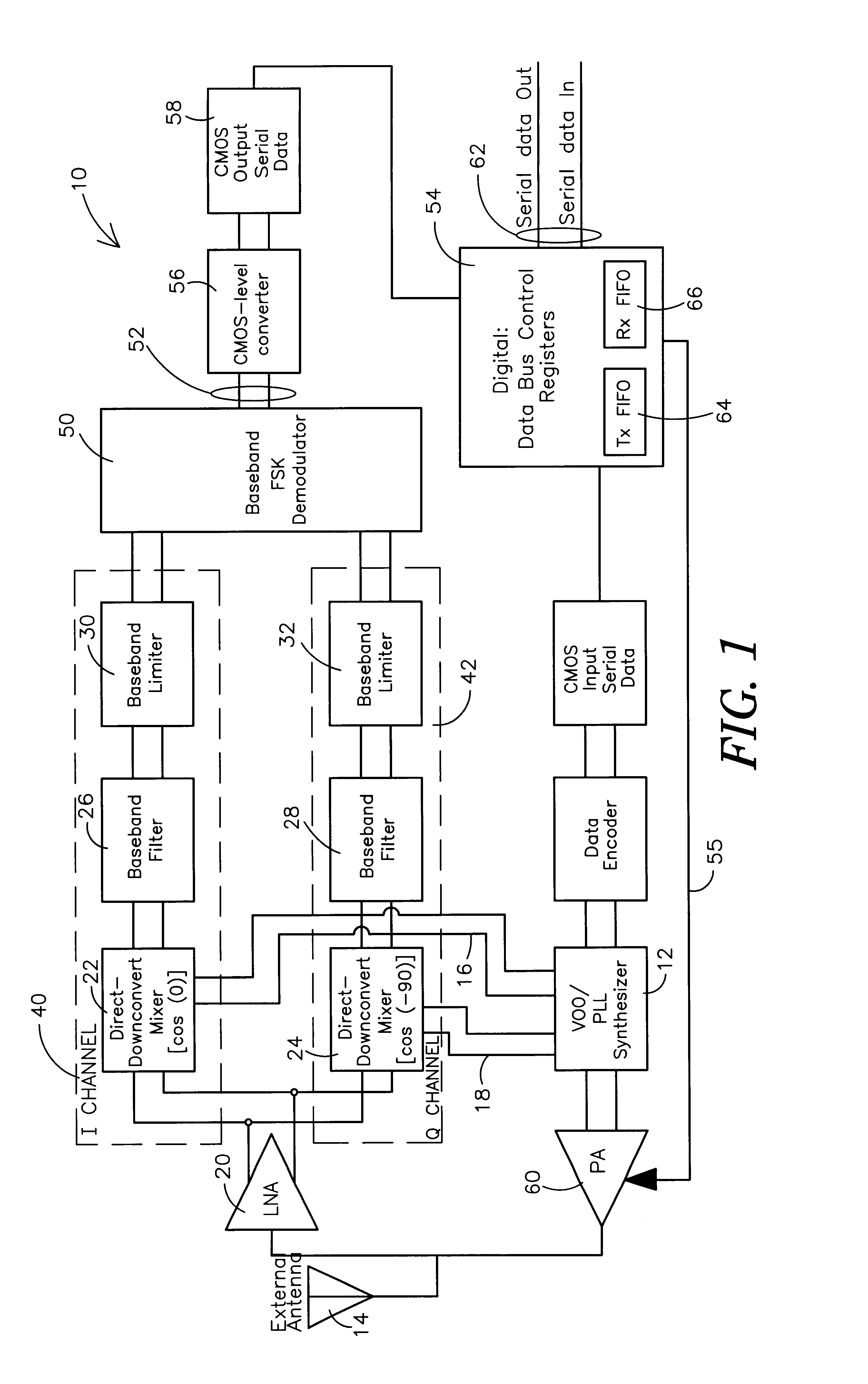
[0033]FIG. 1 is a block diagram of an integrated direct down conversion Narrowband FSK Transceiver 10 that incorporates the present invention. The Narrow Band FSK Transceiver 10 includes both transmit and receive functions, preferably on a single substrate with minimal use of external components. In use, the Narrow Band FSK Transceiver 10 provides a half-duplex transceiver radio data link capable of statistical frequency-spread transmissions.

[0034]Two or more Narrow Band Transceivers 10 can be used to form a wireless data communication network. Because each Narrowband FSK Transceiver 10...


PUM


Abstract

A compensation circuit is disclosed for compensating bias levels of an operational circuit in response to variations in a supply voltage. The compensation mechanism identifies variations in the supply voltage by comparing the voltage of a selected node of the operation circuit with a relatively constant or fixed reference voltage. Based on the results of the comparison, the compensation mechanism adjusts selected bias levels in the operational circuit, preferably using current stealing circuitry, so that the functionality and performance of the operational circuit can be substantially maintained. A biasing circuit for biasing one or more differential pairs is also disclosed.

Description

CROSS REFERENCE TO CO-PENDING APPLICATIONS[0001]The present application is related to U.S. patent application Ser. No. 09 / 311,242 filed May 13, 1999, entitled “Output Buffer With Independently Controllable Current Mirror Legs”; U.S. patent application Ser. No. 09 / 311,105 filed May 13, 1999, entitled “Differential Filter with Gyrator”; U.S. patent application Ser. No. 09 / 311,246 filed May 13, 1999, entitled “Filter with Controlled Offsets For Active Filter Selectivity and DC Offset Control”; U.S. patent application Ser. No. 09 / 311,092 filed May 13, 1999, entitled “State Validation Using Bi-Directional Wireless Link”; U.S. patent application Ser. No. 09 / 311,250 filed May 13, 1999, entitled “Wireless System With Variable Learned-In Transmit Power”; and U.S. patent application Ser. No. 09 / 311,014 filed May 13, 1999, entitled “Wireless Control Network With Scheduled Time Slots”, all of which are assigned to the assignee of the present invention and incorporated herein by reference.BACKGR...

Claims


Application Information

Patent Timeline
Patent Type & Authority Patents(United States)
IPC IPC(8): H03F3/45H03F1/30H03F3/193
CPCH03F3/45479H03F2200/294H03F2200/372
Inventor TANJI, TODD M.WENTINK, ROBERT S.
Owner HONEYWELL INC
Why Eureka
Try Eureka