Process for fabricating a leadless plastic chip carrier

a leadless plastic and chip carrier technology, applied in the direction of printed circuit manufacturing, printed circuit non-printed electric components association, basic electric elements, etc., can solve the problems of limiting the packaging density of such prior art devices, time-consuming and relatively expensive deposition of successive layers of metal, etc., and achieves material cost savings and robust three-dimensional structure

Inactive Publication Date: 2005-09-20
UTAC HEADQUARTERS PTE LTD
View PDF31 Cites 186 Cited by
  • Summary
  • Abstract
  • Description
  • Claims
  • Application Information

AI Technical Summary

Benefits of technology

[0016]Advantageously, a robust three dimensional structure results from laminating a pair of strips of copper and selectively etching back the copper to leave the die attach pad, the power ring and the I/O contacts. The process therefore

Problems solved by technology

The inner leads terminate in outer leads that are bent down to contact a mother board, thereby limiting the packaging density of such prior art devices.
The depos

Method used


Image

  • Process for fabricating a leadless plastic chip carrier
  • Process for fabricating a leadless plastic chip carrier
  • Process for fabricating a leadless plastic chip carrier

Examples


first embodiment

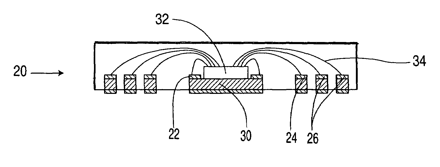
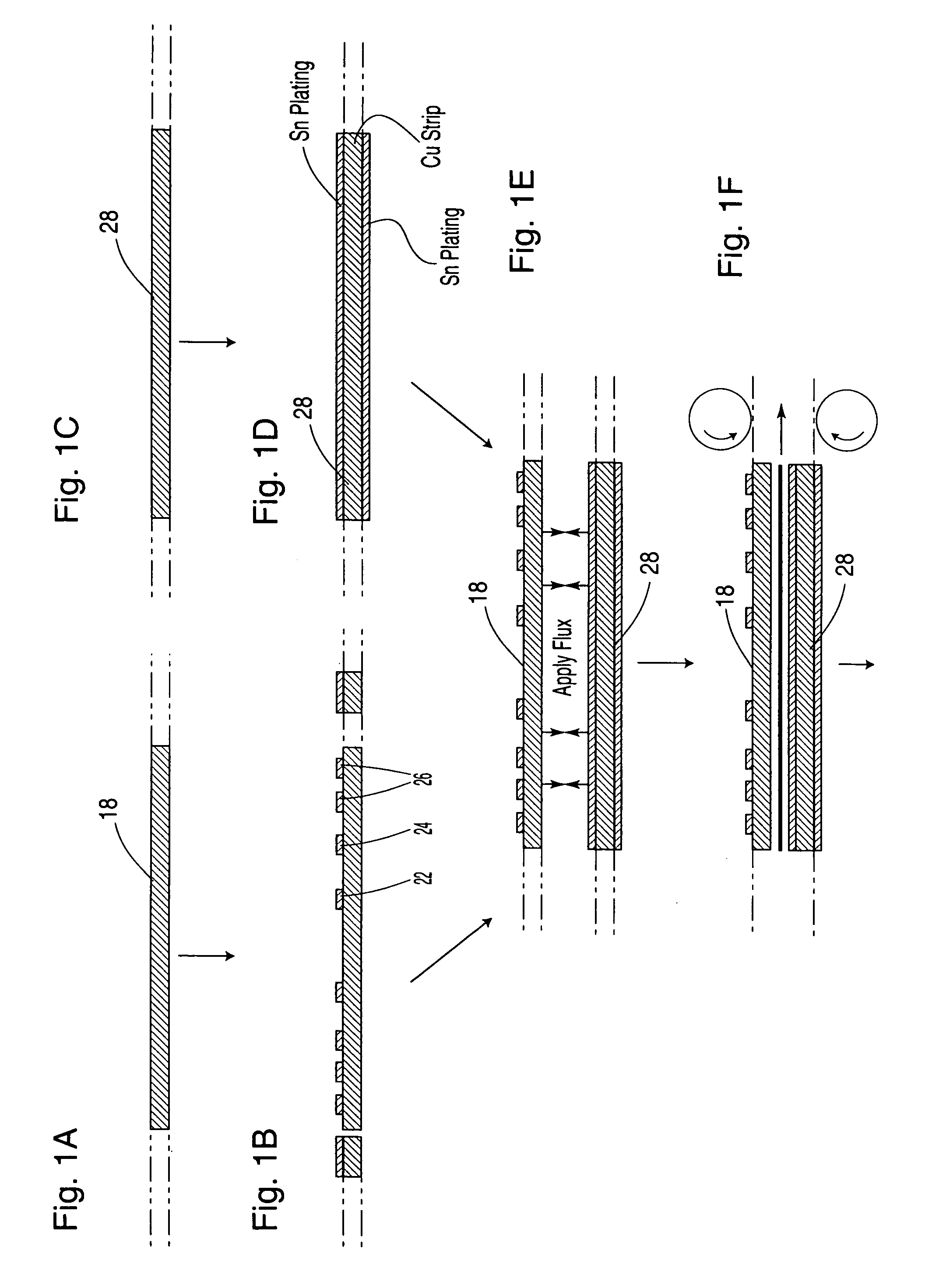
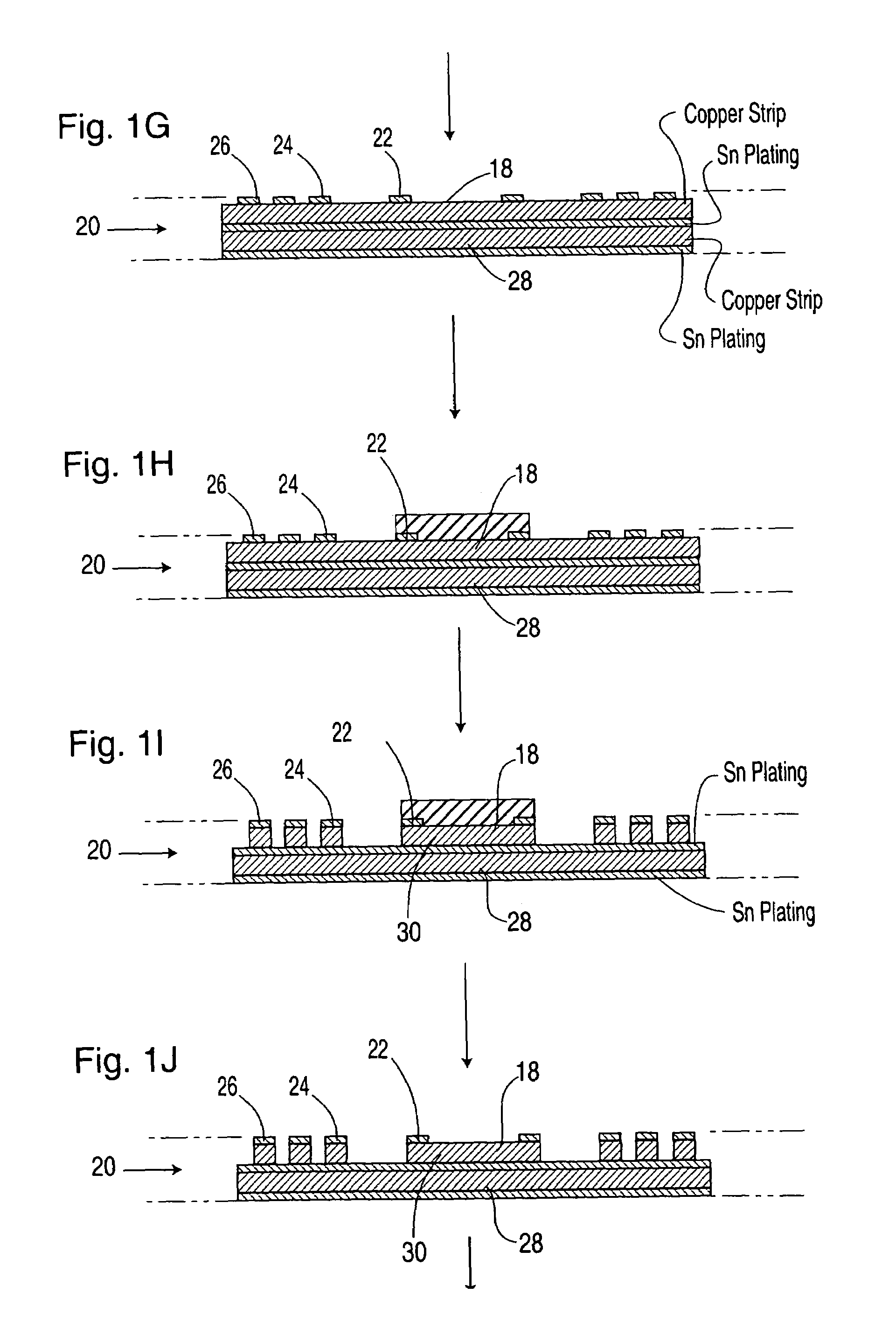
[0023]Reference is made to FIGS. 1A to 1L which show the process for manufacturing a leadless plastic chip carrier (LPCC) according to the present invention. Referring first to FIG. 1A, an elevation view is provided of a first metal strip 18 that forms a part of the raw material of the leadframe strip (indicated generally by the numeral 20 in FIG. 1G). In the present embodiment, the metal strip 18 is a copper strip. As discussed in greater detail in Applicant's own U.S. Pat. No. 6,299,200, issued May 8, 2001, the contents of which are incorporated herein by reference, the leadframe strip 20 is divided into a plurality of sections. Each of the sections incorporates a plurality of leadframe units in an array (e.g. 3×3 array, 5×5 array, etc.). Only one such unit is depicted in the elevation views of the Figures, portions of adjacent units being shown by stippled lines.

[0024]The metal strip 18 is selectively plated with a preplating metal using plating resist to define the plating areas...

second embodiment

[0035]Reference is now made to FIGS. 2A–2O which show a process for manufacturing a Leadless Plastic Chip Carrier (LPCC), according to the invention. Referring to FIG. 2A, an elevation view is provided of a first metal strip 18 that forms a part of the raw material of the leadframe strip (indicated generally by the numeral 20 in FIG. 2F).

[0036]Referring to FIG. 2B, an elevation view is provided of a second metal strip 28 that forms a second part of the raw material of the leadframe strip 20. The second metal strip 28 is similar to the first metal strip 18 and therefore need not be further described herein. Similar to the first embodiment, the second copper strip 28 of the present embodiment is plated with tin (Sn) or solder on both upper and lower surfaces thereof (FIG. 2C). The coating serves to enhance lamination and etching resist.

[0037]Next, a solder flux is applied to the top, tin-plated surface of the second metal strip 28 (FIG. 2D). Alternatively, flux is applied to the botto...

third embodiment

[0042]Reference is now made to FIGS. 4A to 4M to describe a process for manufacturing a LPCC according to the present invention. Referring first to FIG. 4A, an elevation view is provided of a first metal strip 18 that forms part of the raw material of the leadframe strip (indicated generally by the numeral 20 in FIG. 4G). In the present embodiment, the metal strip 18 is a copper strip.

[0043]The metal strip 18 is selectively plated with a preplating metal using plating resist to define the plating areas. As previously described, the preplating metal is preferably silver (Ag), nickel and gold (Ni / Au) or nickel and palladium (Ni / Pd) (FIG. 4B). The preplating metal is selectively plated in a pattern of a power ring 24, and contact or I / O pads 26. Note that no ground ring is provided in the present embodiment.

[0044]Referring to FIG. 4C, an elevation view is provided of a second metal strip 28 that forms a second part of the raw material of the leadframe strip 20. In the present embodimen...


PUM


Abstract

A process for fabricating a leadless plastic chip carrier includes laminating a first metal strip to a second metal strip to form a leadframe strip, selectively etching the first metal strip to define at least a row of contact pads, mounting a semiconductor die to either a die attach pad or the second metal strip and wire bonding the semiconductor die to ones of the contact pads, encapsulating a top surface of the leadframe strip in a molding material, removing the second metal strip, thereby exposing the die attach pad and the at least one row of contact pads, and singulating the leadless plastic chip carrier from the leadframe strip.

Description

CROSS REFERENCE TO RELATED APPLICATION[0001]This is a continuation-in-part of U.S. patent application Ser. No. 09 / 802,678, filed Mar. 9, 2001, which is a continuation-in-part of U.S. patent application Ser. No. 09 / 288,352 filed Apr. 8, 1999, now U.S. Pat. No. 6,498,099, issued Dec. 24, 2002, which is a continuation-in-part of U.S. patent application Ser. No. 09 / 095,803 filed Jun. 10, 1998, now U.S. Pat. No. 6,229,200, issued May 8, 2001.FIELD OF THE INVENTION[0002]The present invention relates in general to integrated circuit packaging, and more particularly to an improved process for fabricating a leadless plastic chip carrier.BACKGROUND OF THE INVENTION[0003]According to well known prior art IC (integrated circuit) packaging methodologies, semiconductor dice are singulated and mounted using epoxy or other conventional means onto respective die attach pads (attach paddles) of a leadframe strip. Traditional QFP (Quad Flat Pack) packages incorporate inner leads which function as land...

Claims


Application Information

Patent Timeline
IPC IPC(8): H01L21/02H01L21/44H01L21/48H01L21/68H01L23/31H05K1/18H05K3/20
CPCH01L21/4832H01L21/568H01L21/6835H01L23/3107H01L2224/48091H01L2224/48247H01L2924/01046H01L2924/01078H01L2924/01079H01L2924/19041H05K1/185H05K1/187H05K3/205H01L2924/00014H01L24/48H01L2224/48257H01L2224/45144H01L2924/00H01L2224/45124H01L2224/45147H01L24/45H01L2924/14H01L2924/181H01L2924/18165H01L2924/00015H01L2224/05599H01L2924/00012
Inventor MCLELLAN, NEILFAN, CHUN HOKWAN, KIN PUILAU, WING HIM
Owner UTAC HEADQUARTERS PTE LTD
Why Eureka
Try Eureka