

Method for forming, by CVD, nanostructures of semi-conductor material of homogenous and controlled size on dielectric material
a technology of dielectric material and nanostructure, which is applied in the direction of nanotechnology, crystal growth process, chemical vapor deposition coating, etc., can solve the problems of affecting the correct operation of the device, affecting the quality and performance of the device based on the structure, and high dispersion in size, around 50%,
- Summary
- Abstract
- Description
- Claims
- Application Information
AI Technical Summary
Benefits of technology
Problems solved by technology
Method used
Image

Examples
first embodiment
[0022] the first and second semi-conductor materials are in silicon.
second embodiment
[0023] the first semi-conductor material is in silicon and the second semi-conductor material is in germanium.
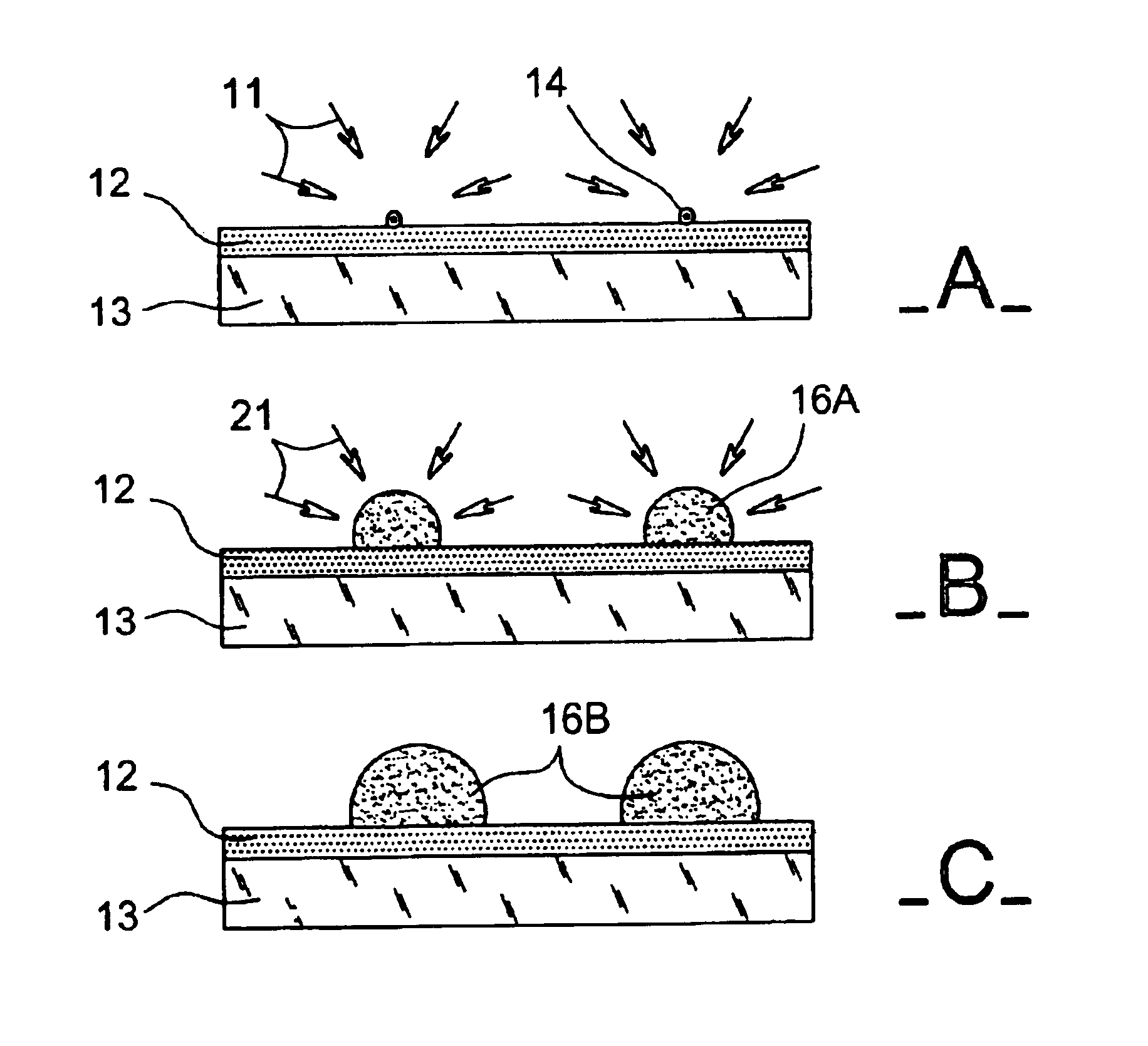
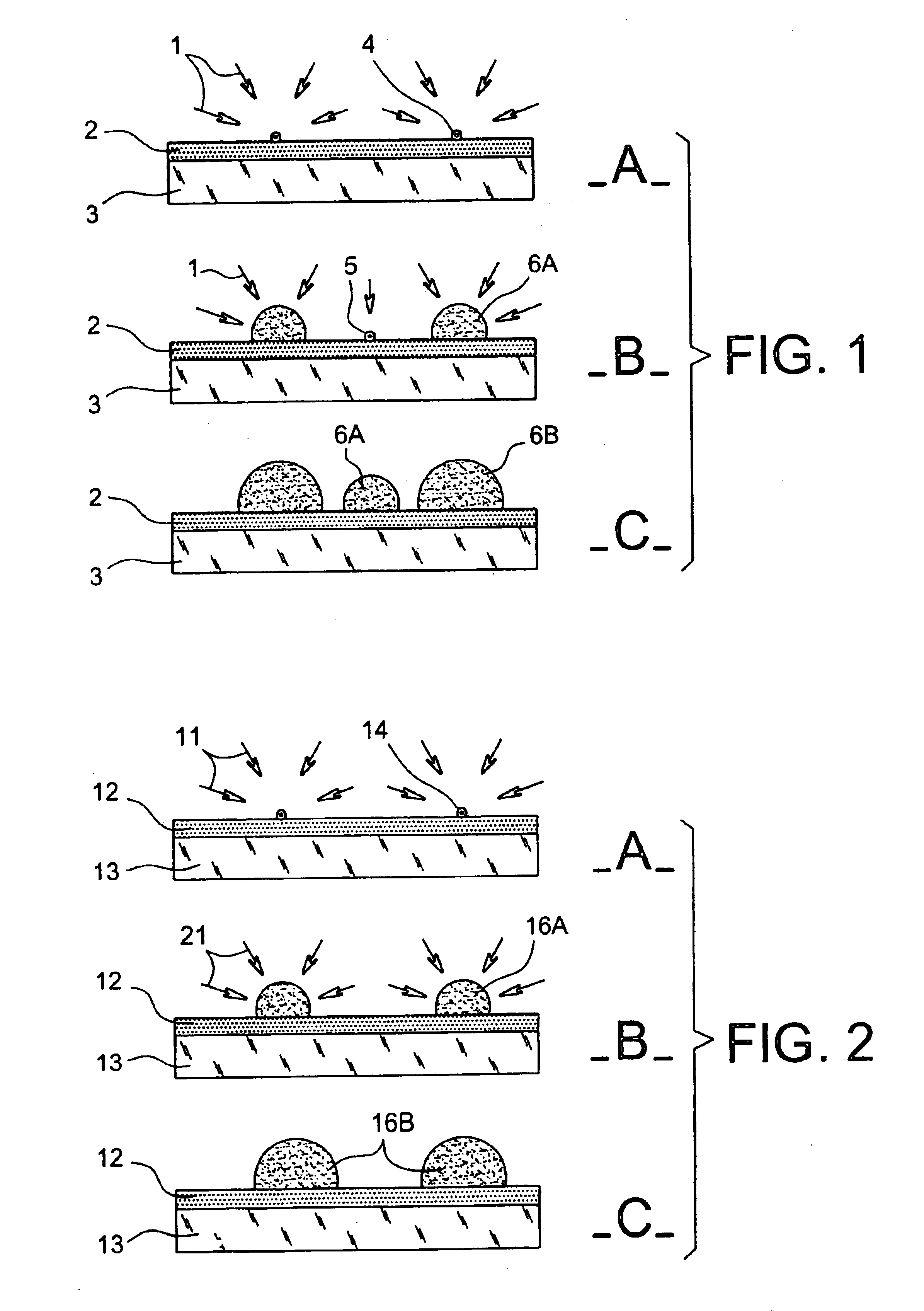
[0024]In other words, the method according to the invention makes it possible, firstly, to deposit nanostructures of germanium isolated from each other on a dielectric material by CVD; if the substrate of dielectric material is in silica and one uses germane as precursor of germanium, one does not need, thanks to said method, to deposit an intermediate continuous layer of silicon on the substrate of dielectric material of silica. By said method, the nanostructures have a homogeneous and controlled size, and their density varies between 109 and some 1012 / cm2. Advantageously, by playing on the temperature and pressure parameters of the precursor during the deposition, one can obtain either crystalline or amorphous nanostructures.
[0025]Furthermore, the invention also makes it possible to deposit, on a dielectric material, nanostructures of silicon isolated from each other by CV...
PUM
| Property | Measurement | Unit |
|---|---|---|
| temperature | aaaaa | aaaaa |
| temperature | aaaaa | aaaaa |
| partial pressures | aaaaa | aaaaa |
Abstract
Description
Claims
Application Information