Image sensor and method for driving an image sensor for reducing fixed pattern noise

a technology of image sensor and fixed pattern, which is applied in the direction of color signal processing circuit, television system, radio control device, etc., can solve the problems of increased cost required for system design and manufacture, difficult to remove inter-chip fpn arising from the offset of output buffer amplifier, and above-mentioned s-n method is not effective for inter-chip fpn, etc., to achieve the effect of removing individual differences of image sensor assemblies and adjusting gain

Inactive Publication Date: 2005-09-27
CANON KK
View PDF32 Cites 23 Cited by
  • Summary
  • Abstract
  • Description
  • Claims
  • Application Information

AI Technical Summary

Benefits of technology

[0024]It is an object of the present invention to provide a high-performance image sensor which can remove FPN arising from inter-chip variations and does not require any dark correction.
[0025]It is another object of the present invention to provide an inexpensive image sensor which can obviate the need for any dark correction means, and can avoid an increase in cost resulting from an increase in chip area, which is inevitable in the prior art.
[0026]It is still another object of the present invention to provide a drive method that can remove inter-chip FPN in an image sensor.
[0027]It is still another object of the present invention to provide an image sensor and its drive method, which can simultaneously remove intra-chip FPN and inter-chip FPN.
[0032]It is still another object of the present invention to provide an image sensor which can adjust gain and can remove individual differences of image sensor assemblies, and its drive method.

Problems solved by technology

The above-mentioned S-N method is not effective for inter-chip FPN.
However, the present inventors found that it is difficult to remove inter-chip FPN arising from the offsets of the output buffer amplifier 36 even by the prior art technique shown in FIG. 1A.
Hence, when a high-gradation image is to be obtained using the conventional image sensor, dark correction is required in units of chips to assure its dynamic range, and the cost required for system design and manufacture increases.
For this reason, the chip area for the analog circuit portion increases, and it is hard to reduce cost.
Furthermore, each sensor chip includes both a digital circuit such as MOS transistors for light signal read and reset, and the aforementioned analog circuit, and the sensor output is readily influenced by noise produced by the digital circuit.

Method used


Image

  • Image sensor and method for driving an image sensor for reducing fixed pattern noise
  • Image sensor and method for driving an image sensor for reducing fixed pattern noise
  • Image sensor and method for driving an image sensor for reducing fixed pattern noise

Examples


first embodiment

Modification of First Embodiment

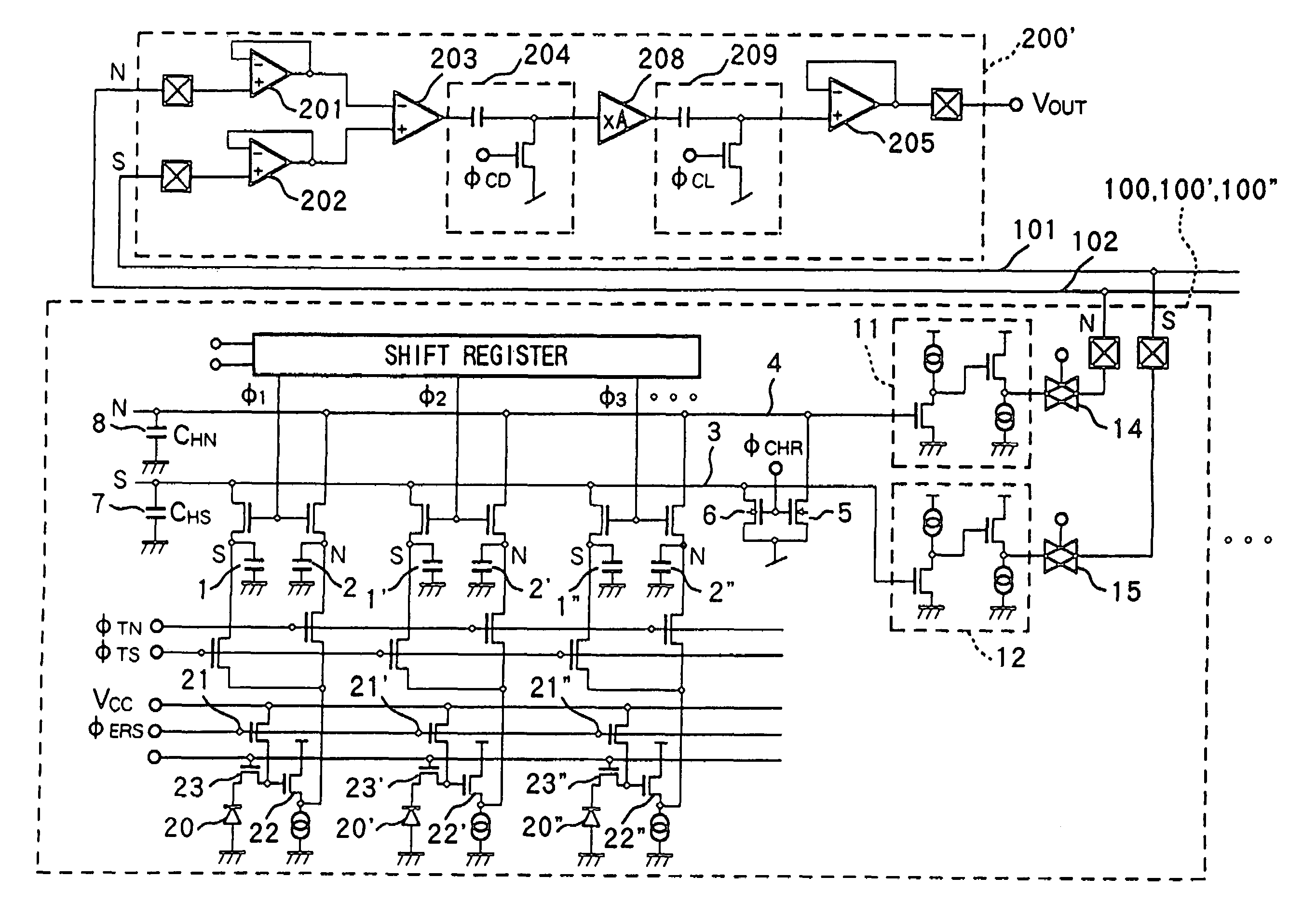
[0078]In the image sensor assembly 300 of the first embodiment, when the power supply for the sensor chips 100, 100′, 100″, . . . and that for the amplifier chip 200 are independently set, a broad dynamic range of the output can be maintained even when the sensor power supply voltage is decreased.

[0079]In the first embodiment, a contact image sensor using a plurality of line sensor chips has been exemplified. However, the present invention is not limited to such specific sensor, but may be effective for a two-dimensional area sensor including a large number of sensor chips. Especially, when area chips in small regions have different photo-electric conversion sensitivities, FPN variations become more conspicuous than a 1-line contact sensor and, hence, it is very effective to apply the present invention.

[0080]As another modification, when an amplification function is added to the amplifier chip 200, the amplification function may be added to, e.g., the...

second embodiment

[0082]FIG. 7 is a circuit diagram of an image sensor according to the second embodiment of the present invention. In the second embodiment, photo-electric converters in each of the sensor chips 100, 100′, 100″, . . . of the first embodiment are respectively constructed by photo-diodes 20, 20′, 20″, . . . , reset switches 21, 21′, 21″, . . . , NMOS source-follower transistors 22, 22′, 22″, . . . , transfer switches 23, 23′, 23″, . . . .

[0083]As other building elements of the second embodiment, each sensor chip has N signal holders 2, 2′, 2″, . . . , S signal holders 1, 1′, 1″, . . . , an N signal output line 4, an S signal output line 3, and reset switches 5 and 6, as in the first embodiment (FIG. 4A).

[0084]The characteristic feature of the second embodiment lies in that the level of a final output VOUT of a sensor assembly 300 can be adjusted by adding a gain amplifier 208 to an amplifier chip 200′. However, when the gain amplifier 208 is added, the output VOUT of the assembly 300 s...

third embodiment

[0099]FIG. 9 is a circuit diagram showing the third embodiment of the present invention. In this embodiment, N and S signals are read out time-serially (i.e., by time division), and the output state of N signals is clamped and is used as a reference signal.

[0100]In the third embodiment, the arrangement of each of the sensor chips 100, 100′, 100″, . . . is substantially the same as that in the second embodiment, i.e., comprises photo-diodes 20, 20′, 20″, . . . , reset switches 21, 21′, 21″, . . . , NMOS source-follower transistors 22, 22′, 22″, . . . , transfer switches 23, 23′, 23″, . . . , N signal holders 2, 2′, 2″, . . . , and S signal holders 1, 1′, 1″, . . . , except that N and S signals are time-serially (time-divisionally) read out onto a single common output line 55. That is, the single common output line 55 is sequentially reset by a reset MOS transistor 56. Since time-division driving is done, the number of source-follower amplifiers 11 including two transistors for amplif...


PUM


Abstract

There is provided a method of driving an image sensor which can remove FPN resulting from inter-chip variations without requiring any dark correction. A semiconductor photosensor chip has a plurality of sensor modules mounted on a mounting substrate, and a semiconductor device in which at least an N signal input buffer circuit for receiving N signals, an S signal input buffer circuit for receiving S signals, a differential circuit for calculating any difference between the outputs from the N and S signal input buffer circuits, and a voltage clamping circuit for clamping the output from the differential circuit are formed on a single semiconductor substrate, and the voltage clamping circuit clamps the reset state of S and N signal common output line.

Description

BACKGROUND OF THE INVENTION[0001]The present invention relates to a method of driving an image sensor (for example, a linear contact image sensor) for reading images in a facsimile, image scanner, digital copying machine, X-ray imaging apparatus, or the like and, more particularly, to removal of fixed pattern noise (FPN) arising from inter-chip differences or deviations in a contact image sensor in which a plurality of semiconductor photosensor chips are mounted on a mounting substrate.[0002]In recent years, in the field of linear photo-electric conversion devices, an equal-magnification (magnification=1) contact image sensor in which a plurality of semiconductor photosensors are mounted has been extensively developed in addition to CCDs using reducing optics.[0003]FIG. 1A is a partial block diagram showing the arrangement of a conventional contact image sensor having an amplifier element, which is disclosed in Journal of Television Society Vol. 47, No. 9 (1993), pp. 1180. In this c...

Claims


Application Information

Patent Timeline
Patent Type & Authority Patents(United States)
IPC IPC(8): H04N5/217H01L27/146H04N1/028H04N5/365H04N5/369H04N5/374H04N5/378
CPCH04N5/3653H04N5/3694H04N5/378H04N25/672H04N25/7013H04N25/75H04N25/60
Inventor KOZUKA, HIRAKU
Owner CANON KK
Why Eureka
Try Eureka