Electrically controlled variable thickness plate

a variable thickness, electric control technology, applied in the direction of optics, instruments, optical elements, etc., can solve the problems of difficult and expensive manufacturing, difficult and expensive to manufacture, and the inability to easily make the optical components and the required electrical actuators very compact in size,

Inactive Publication Date: 2005-09-27
NOKIA CORP
View PDF11 Cites 98 Cited by
  • Summary
  • Abstract
  • Description
  • Claims
  • Application Information

AI Technical Summary

Benefits of technology

[0024]The main purpose of the present invention is to produce a novel device for optical switching, which is based on the use of an electrically deformable viscoelastic layer in order to manipulate the light passing through said viscoelastic layer, but which is not based on using the viscoelastic layer as a grating-like structure. This innovation allowing to manipulate the viscoelastic layer in a completely new way significantly broadens the possibilities to use electrically controlled viscoelastic materials for optical switching applications.
[0029]In one specific embodiment of the invention, the opposite electrode structures and / or substrate materials supporting said structures in the variable thickness plate device are realized as light reflecting structure / s. This causes the light entering the device to pass through the viscoelastic layer more than once and thus makes it possible to create an electrically controlled Fabry Perot Interferometer.
[0030]In another embodiment of the invention, the variable thickness plate device is placed into the optical path of one of the optical arms of a Mach-Zehnder Interferometer. This makes it possible to create an electrically controlled Mach-Zehnder Interferometer type optical switching device. Preferably, and differing from the case of the aforementioned Fabry Perot switch, all the stationary optical surfaces of the variable thickness plate are arranged to have anti-reflection coatings.
[0032]The devices according to the invention are significantly more advantageous than prior art devices in providing much wider possibilities to manufacture electrically controlled optical switching devices. The manufacture of such devices also promises to be relatively easy and economical compared to prior art technologies allowing, for example, the use of a wider variety of substrate materials and simpler manufacturing processes. The manufacture of the devices according to invention do not involve for example the use of environmentally harmful liquid crystal materials, or require deep etching. Further, the optical switching devices according to the invention are independent of polarization.

Problems solved by technology

However, such optical components together with the required electrical actuators cannot be easily made very compact in size and they are also rather difficult and expensive to manufacture, especially as mass-produced articles.
The aforementioned manufacturing process is, however, fairly difficult and thus expensive.
Further, the optical MEMS devices operate mainly only in reflection and thus the capabilities of such devices of more complex transformations of the optical signal / beam and / or its path are limited.
Material fatigue may also become significant in certain applications.
However, because the use of birefringence requires use of polarized light, this severely limits its use as a general method in realizing optical switching devices.
The major drawback of the ESBG technology is the complex manufacturing process required.
This, together with the fact that said devices operate only in reflection, limits the use of such devices due to the limited selection of suitable conductive and reflective materials as well as due to the overall response characteristics (sensitivity to the applied voltages / charges, temporal response characteristics) of the device.

Method used


Image

  • Electrically controlled variable thickness plate
  • Electrically controlled variable thickness plate
  • Electrically controlled variable thickness plate

Examples


Embodiment Construction

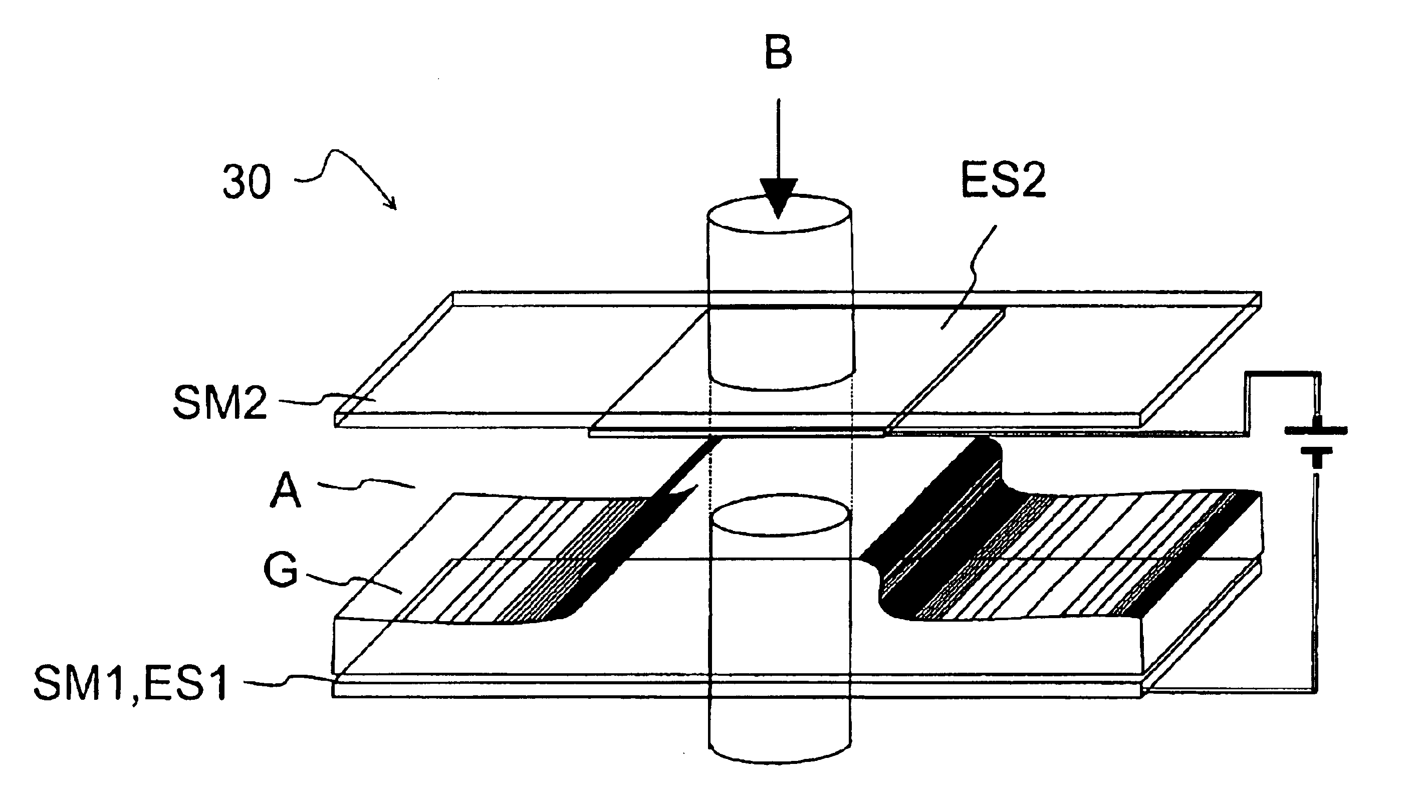
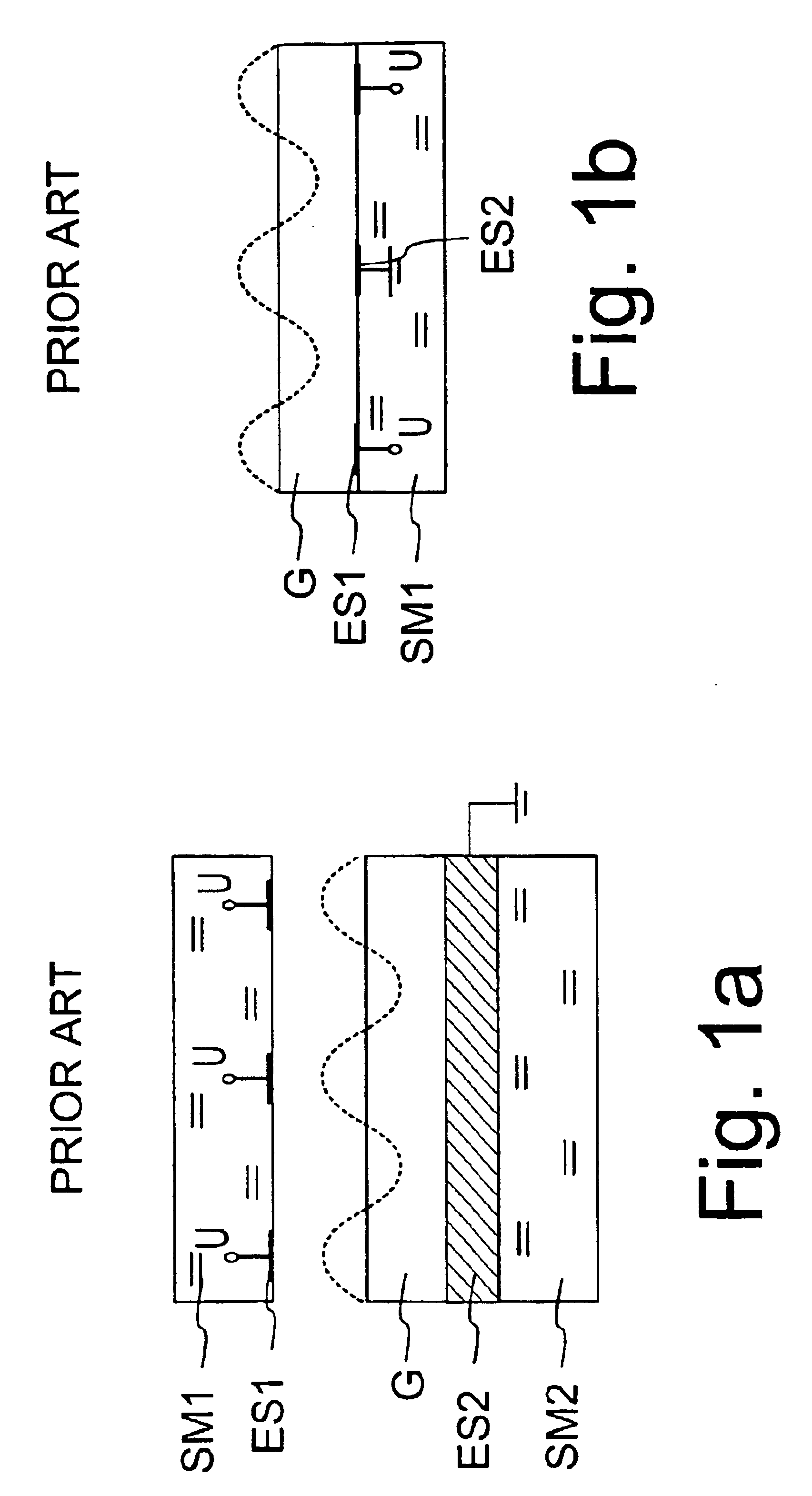
[0040]It is to be understood that the drawings presented hereinbelow are designed solely for purposes of illustration and thus, for example, not for showing the various components of the devices in their correct relative scale and / or shape. For the sake of clarity, the components and details which are not essential in order to explain the spirit of the invention have also been omitted in the drawings.

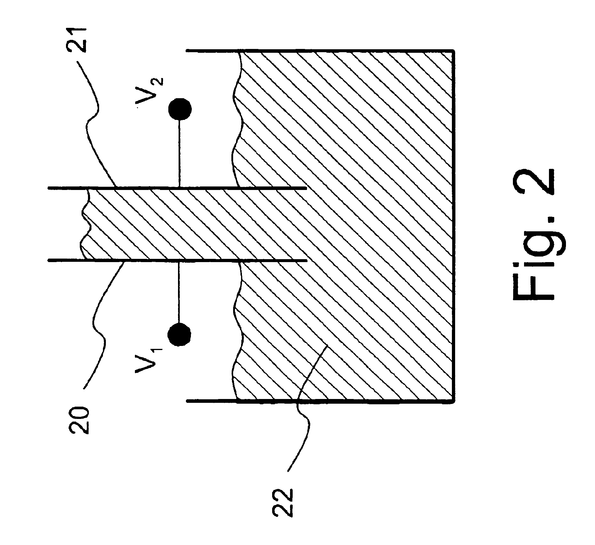
[0041]FIG. 2 illustrates the general principle of physics, which can be observed with dielectric substances. A dielectric substance can be defined as a substance in which an electric field may be maintained with zero or near zero power dissipation, i.e. the electrical conductivity is zero or near zero. In an electric field, the surface of two dielectrics with different dielectric constants is known to experience a force which is proportional to the square of the electric field strength. In FIG. 2 where an electric field is formed between electrode plates 20 and 21 of a field capacitor b...


PUM

PropertyMeasurementUnit
total area A1aaaaaaaaaa
voltageaaaaaaaaaa
voltagesaaaaaaaaaa

Abstract

The invention refers to electrically controlled optical switching devices which are based on the use of a layer of dielectric and transparent viscoelastic material (G) located between transparent first (ES1) and transparent second (ES2) electrode structures. According to the invention, the first (ES1) and second (ES2) electrode structures are arranged in a manner that the thickness of the layer of the viscoelastic material (G) can be electrically altered maintaining the thickness of said layer substantially equal. This makes it possible to realize a generic, electrically controlled variable thickness plate (30). The generic variable thickness plate (30) can be further used to create optical switching devices based on a Fabry Perot Interferometer or a Mach-Zehnder Interferometer.

Description

BACKGROUND OF THE INVENTION[0001]1. Technical Field[0002]The present invention relates to an electrically switchable optical device operating in transmission for manipulating an incident light wave or light waves passing through the device. The invention also relates to a method for forming electrically switchable optical devices for forming such an optical switching device.[0003]2. Discussion of Related Art[0004]Optical signals in different forms are today increasingly utilized in many different types of devices and applications. In order to take full advantage of systems including optical signals or beams, it must be possible to direct the optical signal or beam coming in on a guided optical conduit, or on some other type of optical system in a desired electrically controlled manner to another optical conduit or to another optical system. The aforementioned optical conduit can be, for example, an optical fiber or other type of optical waveguide. There exists a wide variety of opti...

Claims


Application Information

Patent Timeline
Patent Type & Authority Patents(United States)
IPC IPC(8): G02B26/06G02B26/00
CPCG02B26/001G02B26/06
Inventor SCHRADER, MARTIN
Owner NOKIA CORP
Why Eureka
Try Eureka