Electric device, matrix device, electro-optical display device and semiconductor memory having thin-film transistors

a technology of semiconductor memory and matrix device, which is applied in the direction of static indicating device, identification means, instruments, etc., can solve the problems of reducing production yield, complex process, and configuration unsuitable for display devices, and achieves excellent reproducibility and stability of energy levels, and the process itself is quite simple.

Inactive Publication Date: 2005-10-11
SEMICON ENERGY LAB CO LTD
View PDF178 Cites 27 Cited by
  • Summary
  • Abstract
  • Description
  • Claims
  • Application Information

AI Technical Summary

Benefits of technology

[0025]It is an object of the present invention to provide a semiconductor circuit for permitting the use of TFTs producing large leakage currents, by optimizing the design of the circuit; the leakage currents from NMOS devices are not necessarily reduced by controlling the manufacturing process. As described above, where an active layer is formed from a high-purity silicon material, the layer becomes N−-type. Its energy levels are quite excellent in reproducibility and stable. Also, the process itself is quite simple and provides a sufficiently high production yield. On the other hand, in various methods of controlling the threshold value, the process is complicated. Furthermore, the energy levels such as Fermi levels in the obtained active layer vary from lot to lot, thus reducing the production yield.
[0037]Active matrices of liquid-crystal displays and DRAMs are all required to be refreshed. During the refreshing operation, the resistances of TFTs must be large enough to prevent the capacitances of the pixels and the capacitors from being discharged. In this case, if the NMOS TFTs are used, then it is impossible to drive the elements satisfactorily because of large leakage current. In this respect, the use of the PMOS TFTs producing a smaller amount of leakage current yields advantages.

Problems solved by technology

On the other hand, in various methods of controlling the threshold value, the process is complicated.
Furthermore, the energy levels such as Fermi levels in the obtained active layer vary from lot to lot, thus reducing the production yield.
If the NMOS TFTs are inserted in parallel, a large amount of leakage current is produced and so this configuration is unsuited for display devices.

Method used


Image

  • Electric device, matrix device, electro-optical display device and semiconductor memory having thin-film transistors
  • Electric device, matrix device, electro-optical display device and semiconductor memory having thin-film transistors
  • Electric device, matrix device, electro-optical display device and semiconductor memory having thin-film transistors

Examples


example 1

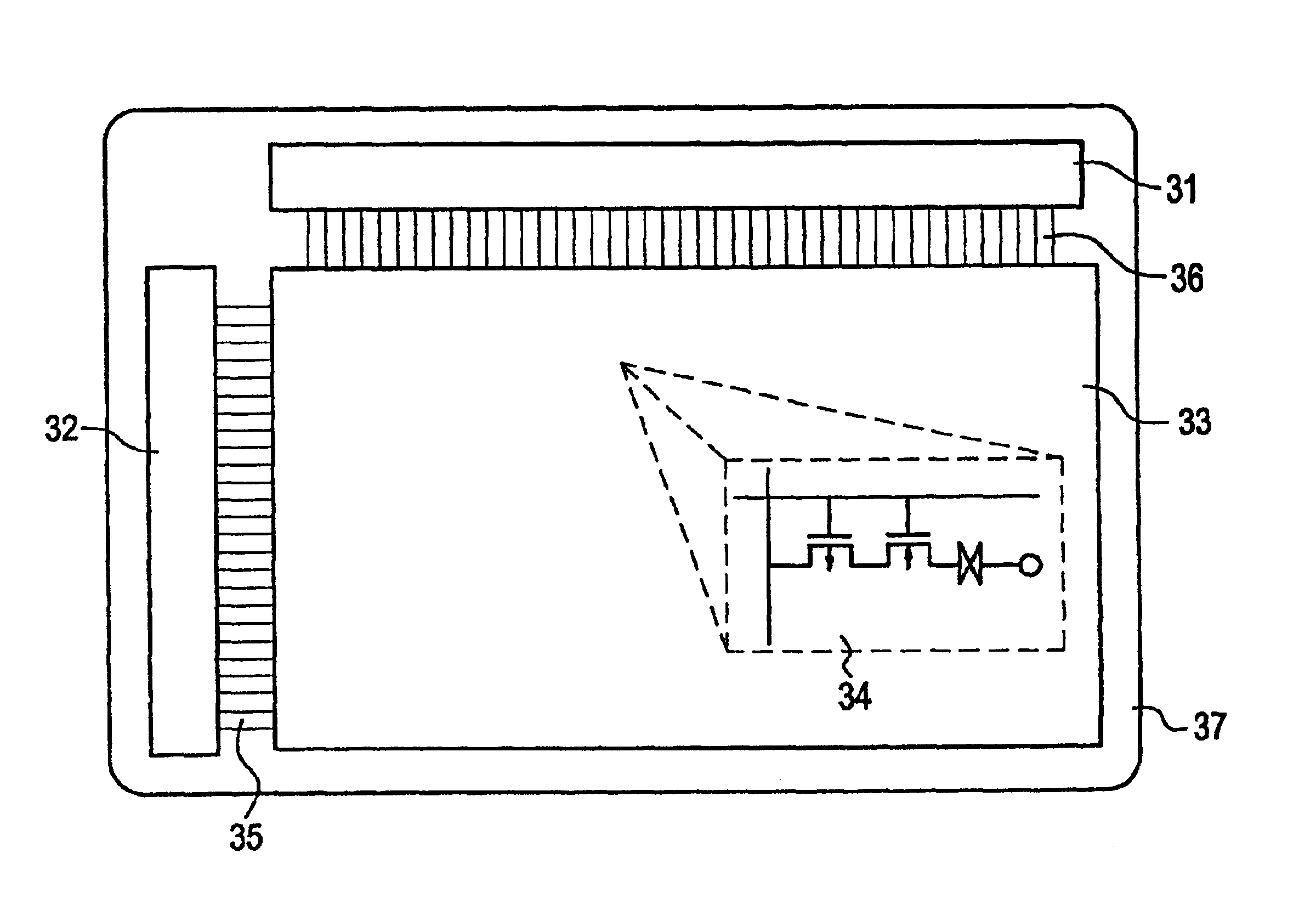
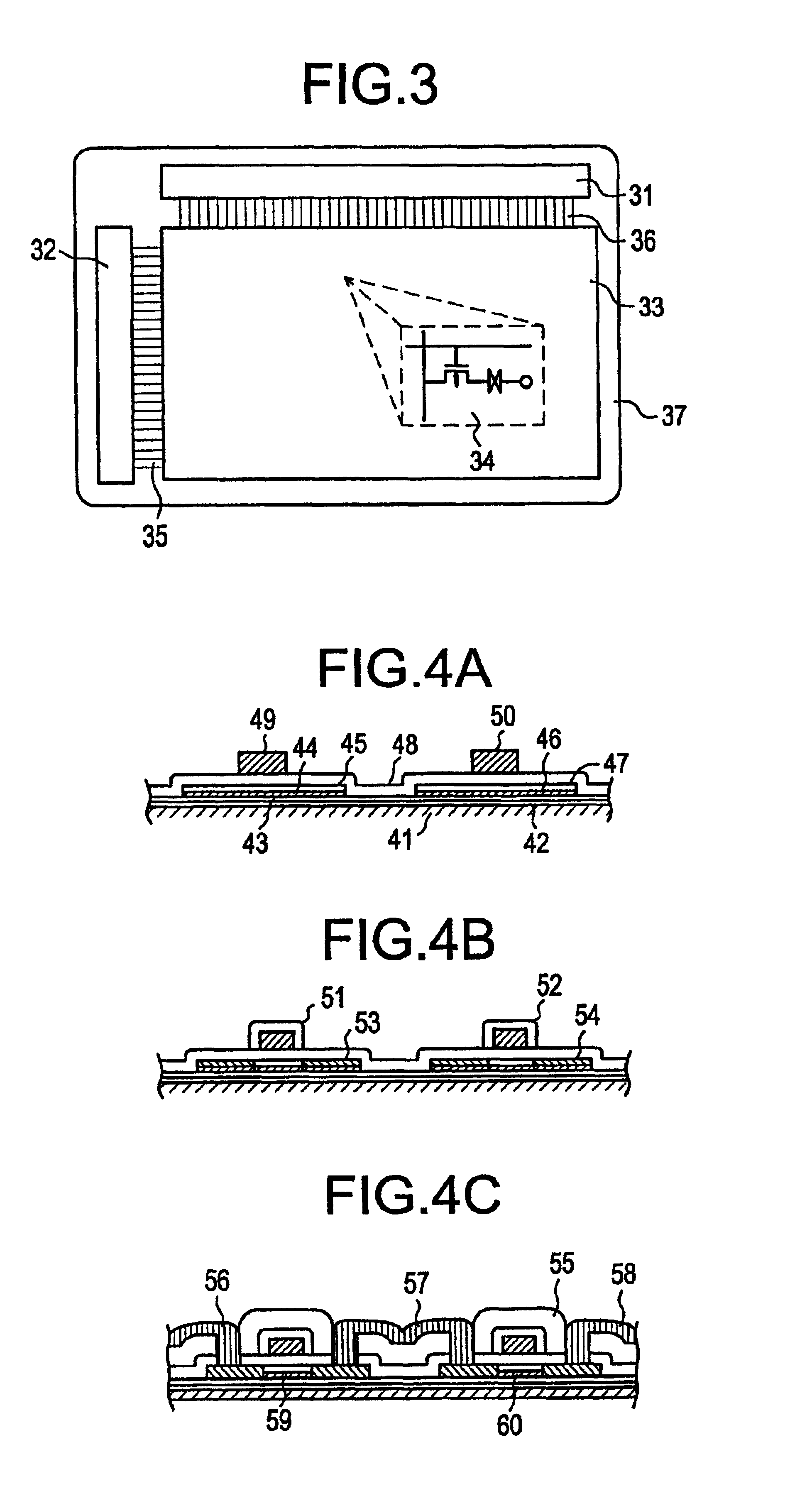
[0057]A CMOS circuit according to this EXAMPLE 1 of the present invention is described below by referring toFIG. 4, (A)-(C). An electric device in accordance with this EXAMPLE 1 is shown in FIG. 6 and comprises a pair of substrates, the CMOS circuit and a pixel electrode provided on one of the substrates, a transparent conductive film 72 provided on the other one of the substrates, and an electro-optical modulating layer 73 provided between the pixel electrode (said one of the substrates) and the transparent conductive film (the other one of the substrates). This circuit comprises a substrate 41 made of #7059 glass manufactured by Corning Co., Ltd. The substrate can be made from various other materials. From whatever material is the substrate made, the substrate must be so processed that no moving ions such as sodium ions enter semiconductor films. An ideal substrate is made of a synthesized quartz having a small alkalinity. If it is difficult to adopt this substrate for economical ...

example 2

[0070]FIG. 5, (A)-(E), illustrate successive steps performed to fabricate NMOS and PMOS devices according to the invention. In the present example, TFTs were fabricated by a high-temperature process. First, an undoped polysilicon film having a thickness of 100 to 500 nm, preferably 150 to 200 nm, was formed on an insulating substrate 61 of quartz by low-pressure CVD. The insulating substrate 61 was 105 mm wide, 105 mm long, and 1.1 mm thick. Then, the polysilicon film was oxidized in a dry, high-temperature oxygen ambient within a temperature range from 850 to 1100° C., preferably from 950 to 1050° C. In this way, a silicon oxide film 62 was formed on the insulating substrate (FIG. 5(A)).

[0071]An amorphous silicon film having a thickness of 100 to 1000 nm, preferably 350 to 700 nm, was formed from disilane by plasma-assisted CVD or low-pressure CVD. The substrate temperature was 350 to 450° C. The laminate was annealed for a long time at a temperature of 550 to 650° C., preferably 5...


PUM

PropertyMeasurementUnit
voltageaaaaaaaaaa
thicknessaaaaaaaaaa
thicknessaaaaaaaaaa

Abstract

A circuit adapted to dynamically activate an electro-optical display device is constructed from a thin-film gate-insulated semiconductor device. This device comprises PMOS TFTs producing only a small amount of leakage current. Besides the dynamic circuit, a CMOS circuit comprising both NMOS and PMOS thin-film transistors is constructed to drive the dynamic circuit.

Description

FIELD OF THE INVENTION[0001]The present invention relates to matrix devices which have a matrix structure, have MOSFETs or MISFETs (collectively referred to as MOS devices) as switching devices, and perform dynamic operation such as liquid-crystal displays and dynamic RAMs (DRAMs). Examples of these matrix devices include electro-optical display devices and semiconductor memories. The invention also relates to a circuit for driving such matrix devices. More particularly, the invention relates to a device using thin-film transistors such as thin-film transistors formed as MOS devices on an insulating substrate.BACKGROUND OF THE INVENTION[0002]Recently, researches have been carried out on insulated-gate semiconductor devices comprising active layers (also known as active regions) in the form of thin films on an insulating substrate. Especially, thin-film insulated-gate transistors, or so-called thin-film transistors (TFTs) have been earnestly investigated. These devices are intended t...

Claims


Application Information

Patent Timeline
Patent Type & Authority Patents(United States)
IPC IPC(8): H01L21/70H01L27/12H01L21/84G02F1/13G02F1/1362G02F1/136G02F1/133G02F1/1368G09F9/35H01L21/00H01L21/02H01L21/336H01L21/77H01L21/8242H01L21/8244H01L27/00H01L27/02H01L27/11H01L29/76H01L29/78H01L29/786H01L29/94H01L31/062H01L31/113H01L31/119
CPCH01L27/1214H01L29/78603H01L29/78609H01L29/78675H01L29/78696G02F1/13454G02F2001/136245H01L27/10873H01L29/78666G02F1/136245H10B12/05
Inventor YAMAZAKI, SHUNPEITAKEMURA, YASUHIKO
Owner SEMICON ENERGY LAB CO LTD
Why Eureka
Try Eureka