Method for manufacturing shallow trench isolation in semiconductor device

a semiconductor device and trench isolation technology, applied in semiconductor/solid-state device manufacturing, basic electric elements, electric devices, etc., can solve the problems of reducing the active area, reducing the design rule, and deteriorating oxide (fox) and other problems, to achieve the effect of preventing the phenomenon of punching and improving the gap-filling property

Active Publication Date: 2005-10-11
SK HYNIX INC
View PDF15 Cites 12 Cited by
  • Summary
  • Abstract
  • Description
  • Claims
  • Application Information

AI Technical Summary

Benefits of technology

[0016]It is, therefore, an object of the present invention to provide a method for manufacturing a shallow trench isolation (STI) in a semiconductor device by employing a nitridation process instead of forming a liner nitride, to thereby improve a gap-fill property and to prevent a punchthrough phenomenon.

Problems solved by technology

The LOCOS technique, however, has several drawbacks that a field oxide (FOX) is deteriorated with a decrease of a design rule and further, a bird's beak structure encroached into an active area of the device, thereby reducing the active area.
Thus, the LOCOS technique is rarely employed to form the isolation region as the device becomes nano-miniaturized nowadays.
The semiconductor device having the conventional STI therein, however, suffers from a drawback that a leakage current may occur due to a punchthrough phenomenon, which is more illustrated in detail as followings.
As the design rule gets smaller, the space between the isolation trench 105 decreases, which results in a bad conformality of the wall oxide thickness along an inner surface of the isolation trench 105 because of an oxidation-induced mechanical stress.
Accordingly, although the STI is formed for isolating each transistor, an adjacent transistor is turned on because of the electrical current (I), thereby increasing an off-state leakage.
In particular, as a design rule decreases in manufacturing the semiconductor device nowadays, a width of the STI becomes also narrow so that the punchthrough phenomenon becomes a more serious problem in the miniaturized semiconductor device.
However, this method shows a poor gap-fill property because the width of the isolation trench 105 becomes narrow and narrow as the thickness of the wall oxide 112 increases.
Furthermore, as the thickness of the wall oxide increases, the aspect ratio also increases, which results in a poor gap-fill property.
This thin gate oxide 218 may increase the likelihood of dielectric breakdown, which can deteriorate the characteristic of the device formed in the active area.
Furthermore, it is difficult to expect a reliable device in the long run.

Method used


Image

  • Method for manufacturing shallow trench isolation in semiconductor device
  • Method for manufacturing shallow trench isolation in semiconductor device
  • Method for manufacturing shallow trench isolation in semiconductor device

Examples


Embodiment Construction

[0025]There are provided in FIGS. 4A to 4D and FIGS. 5A and 5D cross sectional views setting forth a method for manufacturing a shallow trench isolation (STI) in a semiconductor device in accordance with preferred embodiments of the present invention.

[0026]Referring to FIGS. 4A to 4D, there are shown cross sectional views setting forth a method for manufacturing the STI in a semiconductor device in accordance with a first preferred embodiment of the present invention.

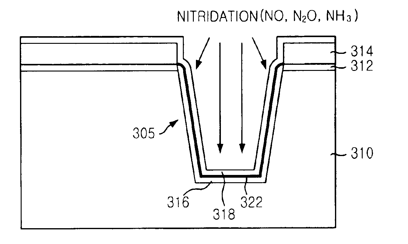
[0027]In FIG. 4A, a first inventive method for manufacturing the STI begins with preparing a semiconductor substrate 310 containing impurities therein obtained by a predetermined process. Thereafter, a pad oxide layer and a pad nitride layer are formed on a top face of the semiconductor substrate 310 in sequence. Subsequently, photoresist masks (not shown) are formed on predetermined locations of the top face of the pad nitride layer. Afterward, the pad nitride layer and the pad oxide layer are patterned into a first pr...


PUM


Abstract

The method for manufacturing an STI in a semiconductor device with an enhanced gap-fill property and leakage property is disclosed by introducing a nitridation process instead of forming a liner nitride. The method includes steps of: preparing a semiconductor substrate obtained by a predetermined process on which a pad oxide and a pad nitride are formed on predetermined locations thereof; forming an isolation trench with a predetermined depth in the semiconductor substrate; forming a wall oxide on the trench; forming a liner oxide on the wall oxide and an exposed surface of the pad nitride; carrying out a nitridation process for forming a nitrided oxide; forming an insulating layer over the resultant structure, wherein the isolation trench is filled with the insulating layer; and planarizing a top face of the insulating layer.

Description

FIELD OF THE INVENTION[0001]The present invention relates to a method for manufacturing a semiconductor device; and, more particularly, to a method for manufacturing a shallow trench isolation (STI) in a semiconductor device by employing a nitridation process instead of forming a liner nitride.DESCRIPTION OF THE PRIOR ART[0002]As it is well known, in a semiconductor device, there is formed an isolation region for electrically isolating elements from each other. In order to form the isolation region, various techniques have been employed such as a local oxidation of silicon (LOCOS) which uses a thermal oxide or a shallow trench isolation (STI) technique which is suitable for a highly integrated circuit device.[0003]The LOCOS technique, however, has several drawbacks that a field oxide (FOX) is deteriorated with a decrease of a design rule and further, a bird's beak structure encroached into an active area of the device, thereby reducing the active area. Thus, the LOCOS technique is r...

Claims


Application Information

Patent Timeline
Patent Type & Authority Patents(United States)
IPC IPC(8): H01L21/70H01L21/762H01L21/76
CPCH01L21/76224H01L21/76
Inventor LIM, JAE-EUNSOHN, YONG-SUN
Owner SK HYNIX INC
Why Eureka
Try Eureka