

Method for forming resist underlayer film, patterning process using the same, and composition for the resist underlayer film
a technology of resist and underlayer film, which is applied in the direction of photosensitive materials, instruments, photomechanical equipment, etc., can solve the problems of etching resistance not only affecting the etching rate but also the surface roughness after etching, and achieve excellent etching resistance, good gap filling characteristics, and high resistance to heat and solven
- Summary
- Abstract
- Description
- Claims
- Application Information
AI Technical Summary
Benefits of technology
Problems solved by technology
Method used
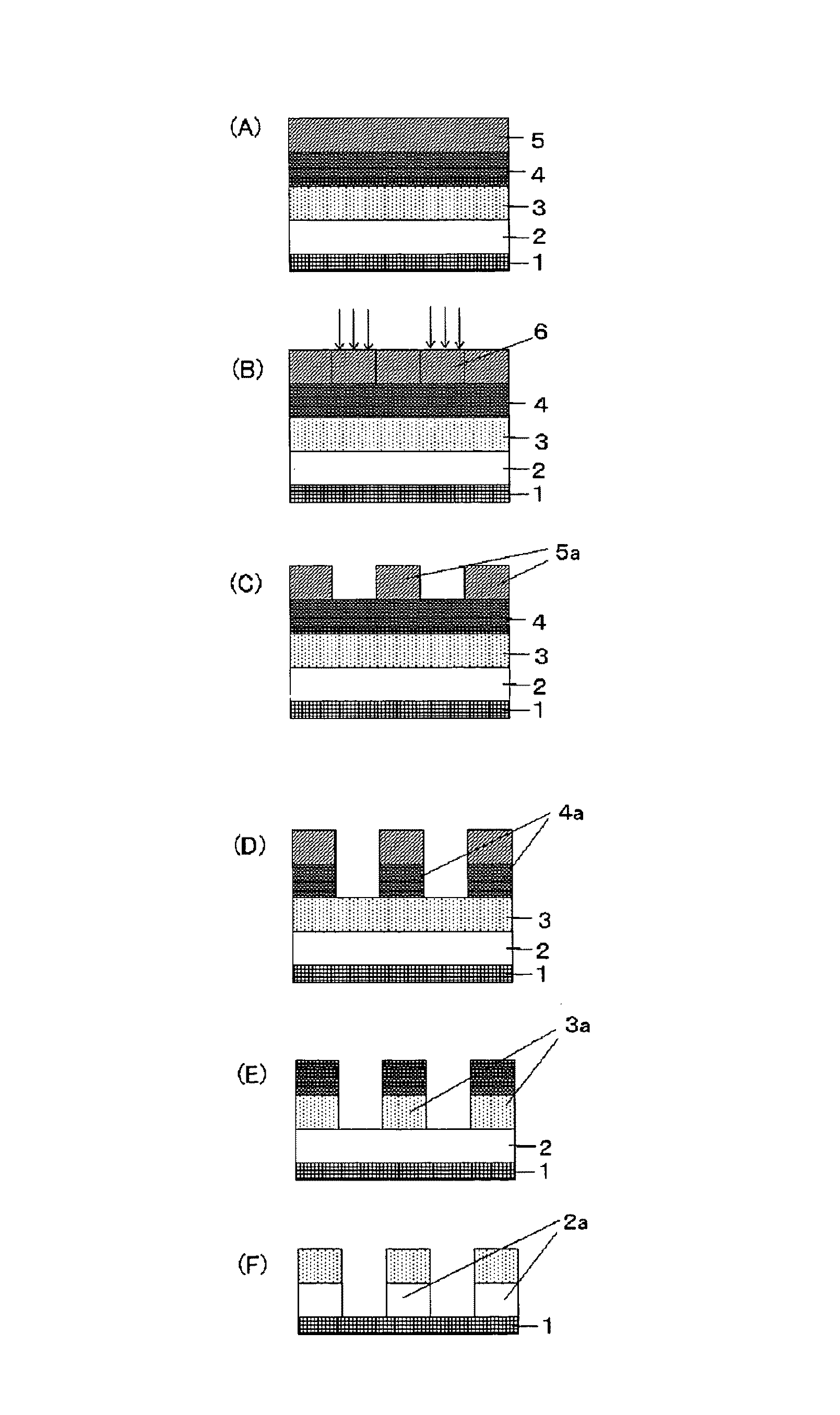
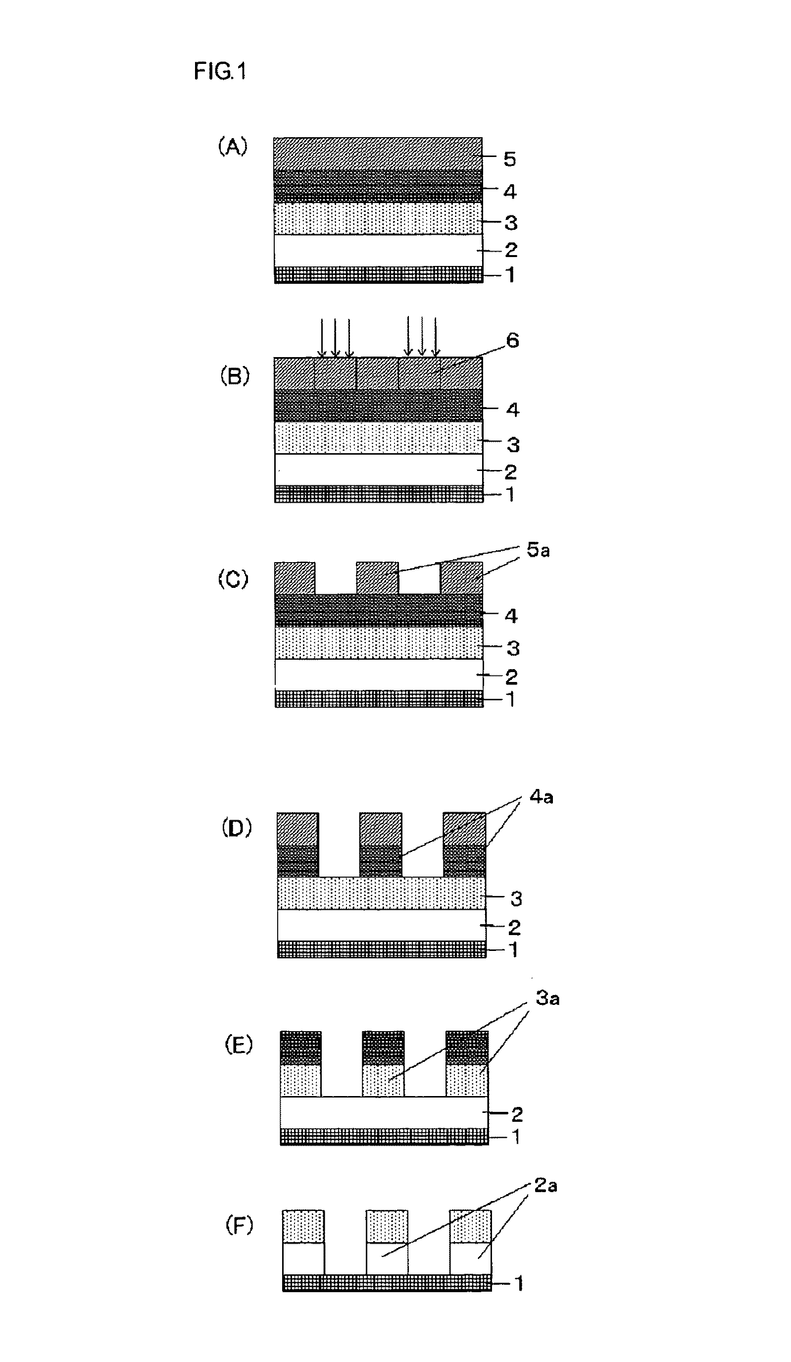
Image

Examples
examples
[0142]Hereinbelow, the present invention will be explained specifically by Examples and Comparative Examples, but the present invention is not restricted by them.
synthesis examples
Polymers 1 to 22 and Comparative Polymers 1 to 3
synthesis example 1
[0143]Into a 300-mL flask were added 291 g of fluorene bisnaphthol, 75 g of 37% aqueous formalin solution, and 5 g of oxalic acid, and then they were heated with stirring at 100° C. for 24 hours. After the reaction, the resulting mixture was dissolved in 500 mL of methyl isobutyl ketone, and then washed thoroughly by water to remove a catalyst and metallic impurities. The solvent was removed by under reduced pressure, and then water and unreacted monomers were removed by reducing the pressure of the system to 2 mmHg at 150° C. to obtain Polymer 1.
[0144]Molecular weight (Mw) and dispersivity (Mw / Mn) were obtained from GPC, and a ratio of components in the polymer was obtained from 1H-NMR-analysis. The results are as shown below:
[0145]Polymer 1: Mw 3,500, Mw / Mn 4.50
[0146]
PUM
| Property | Measurement | Unit |
|---|---|---|
| temperature | aaaaa | aaaaa |
| temperature | aaaaa | aaaaa |
| reflectance | aaaaa | aaaaa |
Abstract
Description
Claims
Application Information