Flexible skin incorporating MEMS technology

a skin and flexible technology, applied in the field of flexible materials, can solve the problems of poor skin reliability, difficult profiling, and rigidity of the mems device, and achieve the effect of greatly improving the skin reliability

Inactive Publication Date: 2005-10-11
UNIV OF CALIFORNIA LOS ANGELES
View PDF6 Cites 23 Cited by
  • Summary
  • Abstract
  • Description
  • Claims
  • Application Information

AI Technical Summary

Benefits of technology

[0010]The present disclosure provides a flexible MEMS technology to produce “smart skins” with integrated MEMS devices that can be easily affixed to non-planar surfaces.
[0012]The present invention includes a new flexible skin technology that is compatible with both IC and MEMS fabrications. Skin reliability is greatly improved by a strong periphery of the silicon islands formed by vertical reactive ion etching (“RIE”). Moreover, the inventors have realized one embodiment as a 2-D flexible skin integrated with shear stress sensors. These flexible skins can be about 3 cm long and about 1 cm wide, and include about 100 sensors. The skin polyimide is about 17 μm thick and the silicon islands are about 75 μm thick. These skins have been successfully taped on a semi-cylindrical (about 1.3 cm diameter) delta wing leading edge to perform real-time 2-D shear stress profiling. This has allowed experimental real time detection of the air flow boundary layer over the leading edge of a delta wing.

Problems solved by technology

However, such MEMS devices are typically rigid and flat.
Profiling becomes much more difficult if the surface is not flat.
However, large sensor size and difficulty in packaging, i.e., plumbing and wiring, have long been limiting factors to realizing good measurements.
However, this technology needed some major improvements before it could be applied to more complicated sensor systems.
The authors identified a major cause of failure as breaks in thin silicon on the island periphery.
These methods are not an ideal solution for a reliable as well as mass-producible smart skin technology.
A large array of metal temperature sensors can be made in this way, but neither ICs nor silicon MEMS are easily integrated with this approach.
Hence, only limited types of sensors are available using this approach and a hybrid assembly of electronic circuits is not readily avoidable.

Method used


Image

  • Flexible skin incorporating MEMS technology
  • Flexible skin incorporating MEMS technology
  • Flexible skin incorporating MEMS technology

Examples


Embodiment Construction

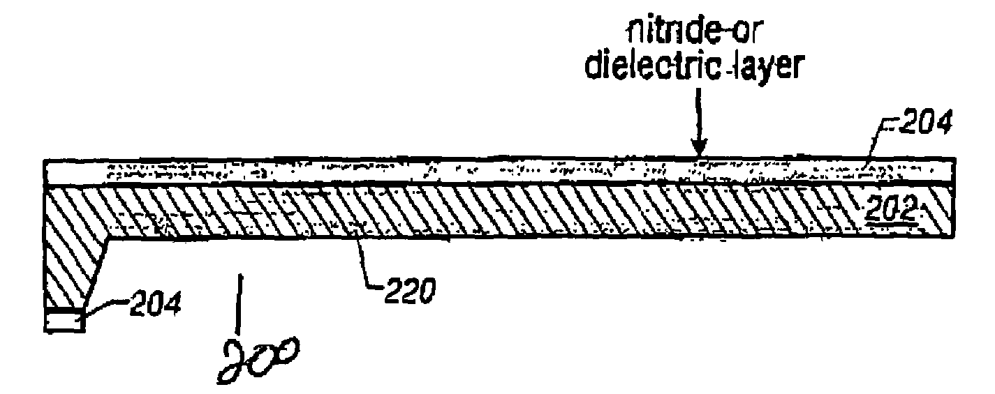
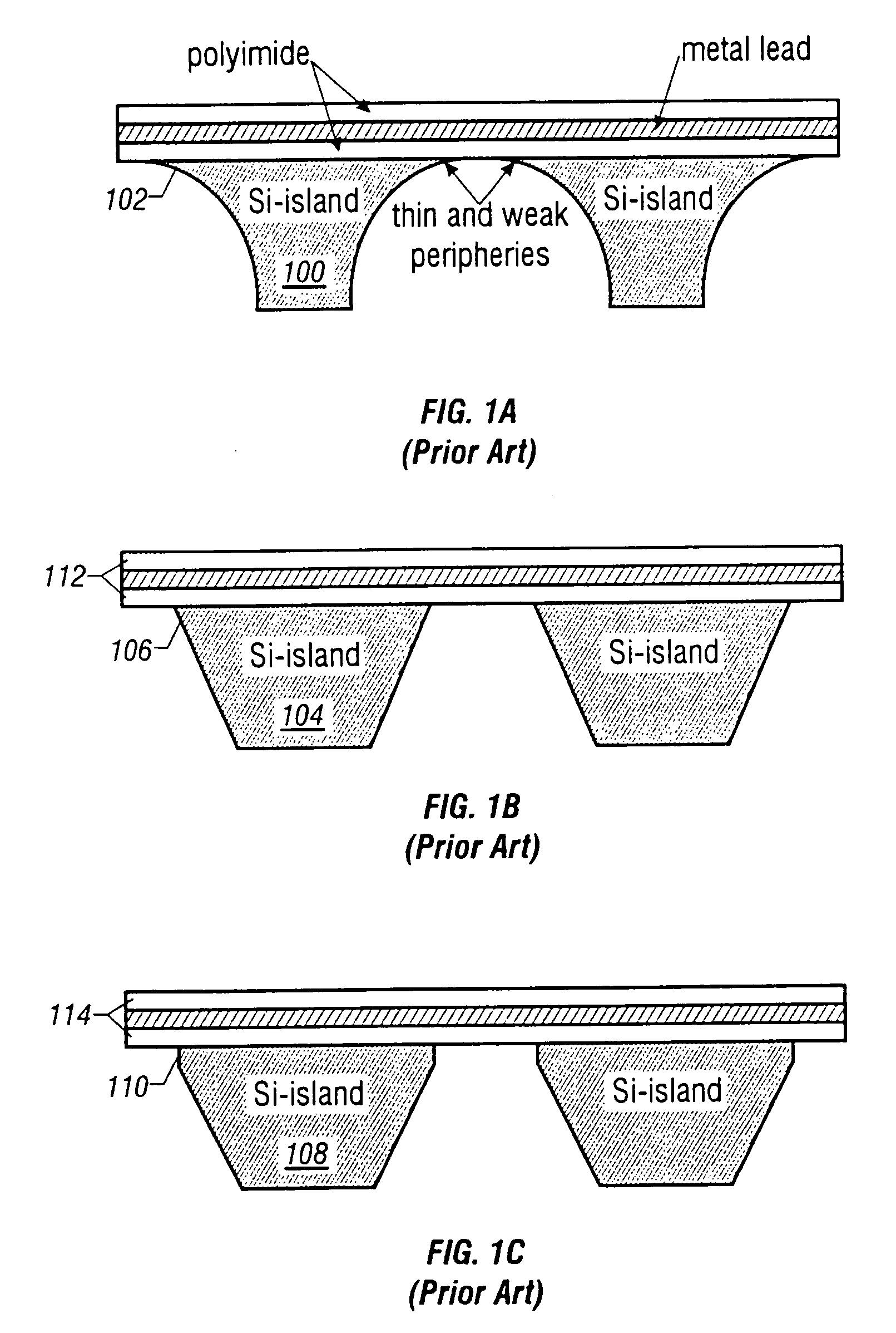
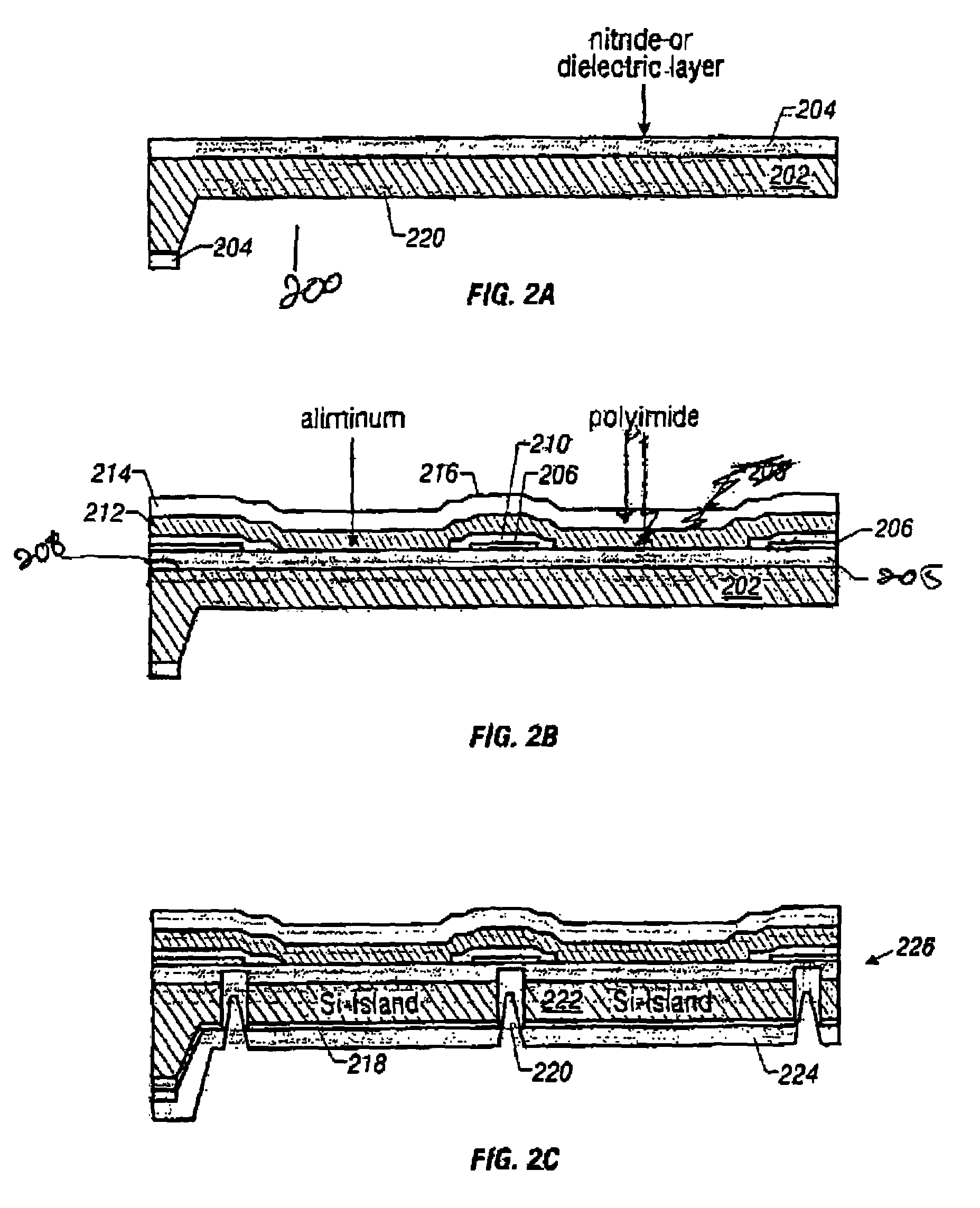
[0022]The inventors believe that many of the failures of flexible skins in prior art systems were caused by thin peripheries on Si islands. These thin peripheries break during squeezing and folding tests. As shown in FIG. 1A, forming Si islands 100 by isotropic HNA etching resulted in thin and weak Si island peripheries 102.

[0023]In comparison, as shown in FIGS. 1B and 1C demonstrate the structural difference that is obtained when etching with caustic anisotropic etchants such as tetramethylammonium hydroxide (“TMAH”) or potassium hydroxide (“KOH”). This etching forms Si islands 104 which are much more robust when subjected to squeezing and folding. The Si islands 104 formed are in a trapezoidal shape. The resulting Si islands 104 have island peripheries 106 that are thicker and stronger than the corresponding island peripheries 102 shown in FIG. 1A. As shown in FIG. 1C, the combination of anisotropic etching and reactive ion etching (“RIE”) results in Si islands 108 which have isla...


PUM

PropertyMeasurementUnit
thickaaaaaaaaaa
thickaaaaaaaaaa
thickaaaaaaaaaa

Abstract

A flexible skin formed of silicon islands encapsulated in a polyimide film. The silicon islands preferably include a MEMS device and are connected together by a polyimide film (preferably about 1–100 μm thick). To create the silicon islands, silicon wafers are etched to a desirable thickness (preferably about 10–500 μm) by Si wet etching and then patterned from the back side by reactive ion etching (RIE).

Description

[0001]This application claims the benefit of U.S. Provisional Application No. 60 / 036,252, filed Jan. 24, 1997. This application is a DIV of Ser. No. 09 / 012,756, now U.S. Pat. No. 6,071,819.[0002]The Government may have certain rights based on Grant No. F49620-94-1-0008 awarded by the U.S. Air Force.FIELD OF THE INVENTION[0003]The invention relates to flexible materials, and more particularly to flexible skins which include microelectromechanical systems (MEMS) devices.BACKGROUND OF THE INVENTION[0004]Microelectromechanical systems (MEMS) devices include semiconductor chips which include microfabricated mechanical systems on the chip, such as sensors.[0005]For some applications, it is desirable to obtain real-time 2-D profiling of certain physical parameters such as temperature, force, pressure or shear stress on a 3-D object. If the surface of the object is flat, this profiling can be achieved by using a monolithic MEMS device with a large amount of sensors. However, such MEMS devic...

Claims


Application Information

Patent Timeline
Patent Type & Authority Patents(United States)
IPC IPC(8): B81B3/00B81B7/00B81C1/00H01L21/301
CPCB81B7/0077B81C1/00246H01L24/24H01L2224/24137
Inventor TAI, YU-CHONGJIANG, FUKANGHO, CHIHMING
Owner UNIV OF CALIFORNIA LOS ANGELES
Why Eureka
Try Eureka