Closed loop residual gas analyzer process control technique

Inactive Publication Date: 2005-10-18
TAIWAN SEMICON MFG CO LTD
View PDF2 Cites 222 Cited by
  • Summary
  • Abstract
  • Description
  • Claims
  • Application Information

AI Technical Summary

Benefits of technology

[0016]A technique for use in fabricating an integrated circuit are disclosed. The method generally begins by performing an operation on a wafer using a fabrication tool. Next, volatiles are desorbed from the wafer. The desorbed volatiles are sampled and raw spectral data indicating the content of the desorbed volatiles is generated. The raw spectral data is subjected to a spectroscopic analysis. An operational parameter of the fabrication tool is then modified responsive to the result of the results

Problems solved by technology

In other words, the materials used or the physical operations employed in the first operation may interfere with, diminish, or destroy the efficacy of the second operation.
If this effect is of sufficient magnitude, a defective device, a defective wafer, or even a batch of defective wafers may result.
If after the CMP operation there is any residual deposited material or any residual slurry or chemical on the wafer, this residual material may interfere with the sputtering process in the PVD system.
This interference may result in an inadequate or incomplete layering of the metal that might render the completed device defective.
This interference may also lead to a host of process control problems.
Exemplary of these process control problems are excessive process, defect and maintenance control variabilities, and inconclusive causation analysis as to what the problem is.
Unfortunatel

Method used


Image

  • Closed loop residual gas analyzer process control technique
  • Closed loop residual gas analyzer process control technique
  • Closed loop residual gas analyzer process control technique

Examples


Embodiment Construction

[0024]Illustrative embodiments of the invention are described below. In the interest of clarity, not all features of an actual implementation are described in this specification. It will of course be appreciated that in the development of any such actual embodiment, numerous implementation-specific decisions must be made to achieve the developers' specific goals, such as compliance with system-related and business-related constraints, which will vary from one implementation to another. Moreover, it will be appreciated that such a development effort, even if complex and time-consuming, would be a routine undertaking for those of ordinary skill in the art having the benefit of this disclosure.

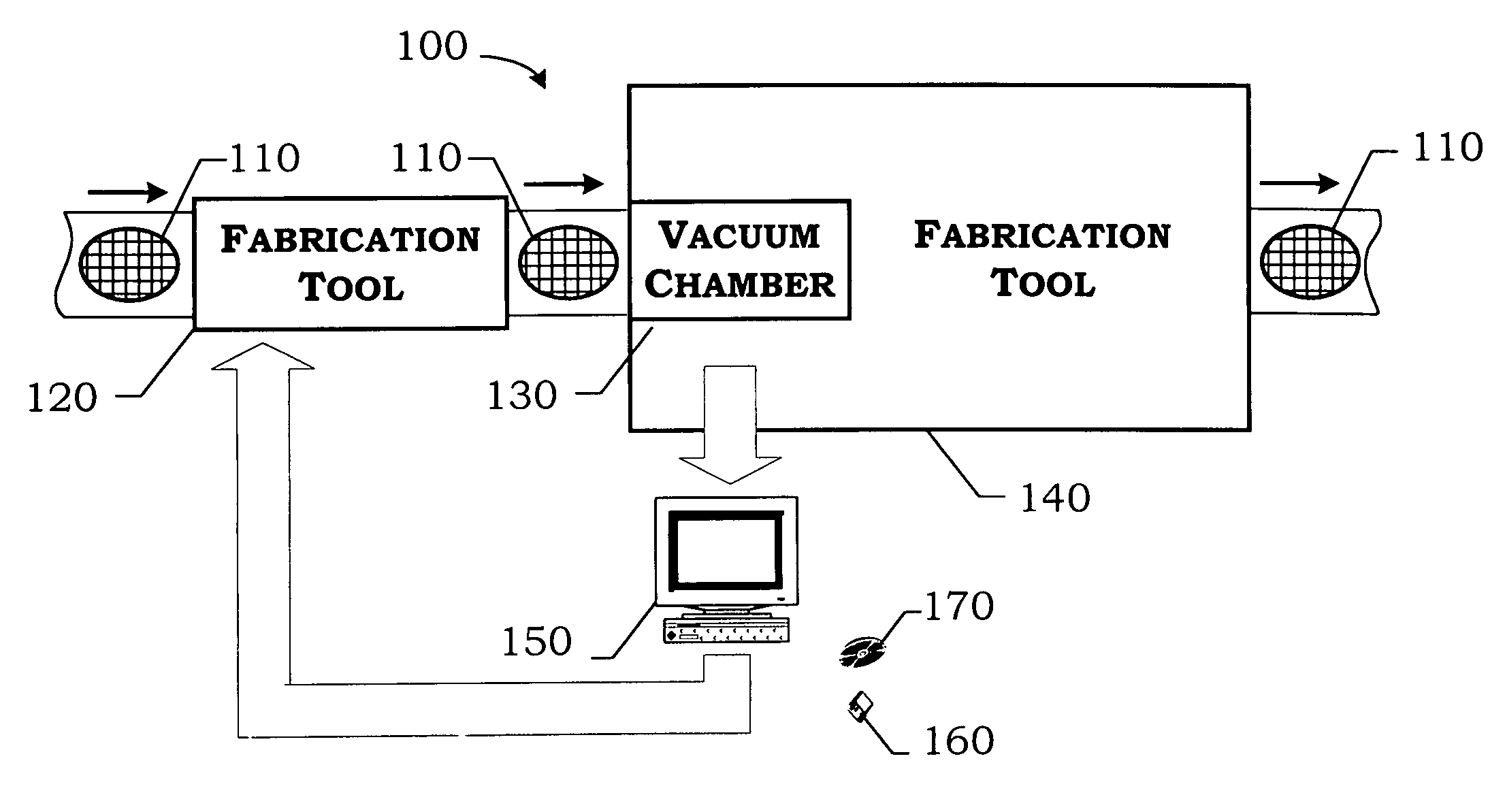
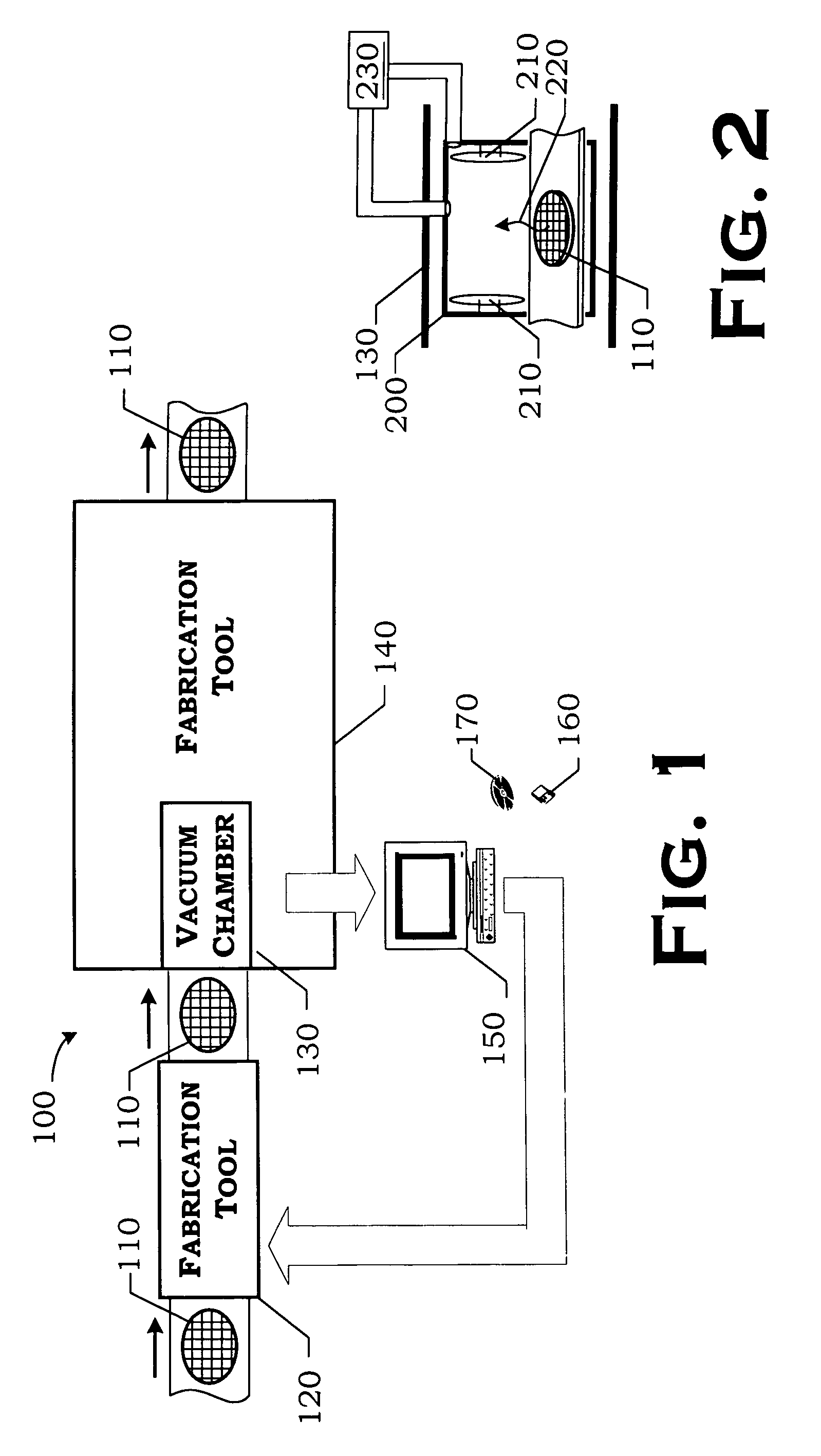
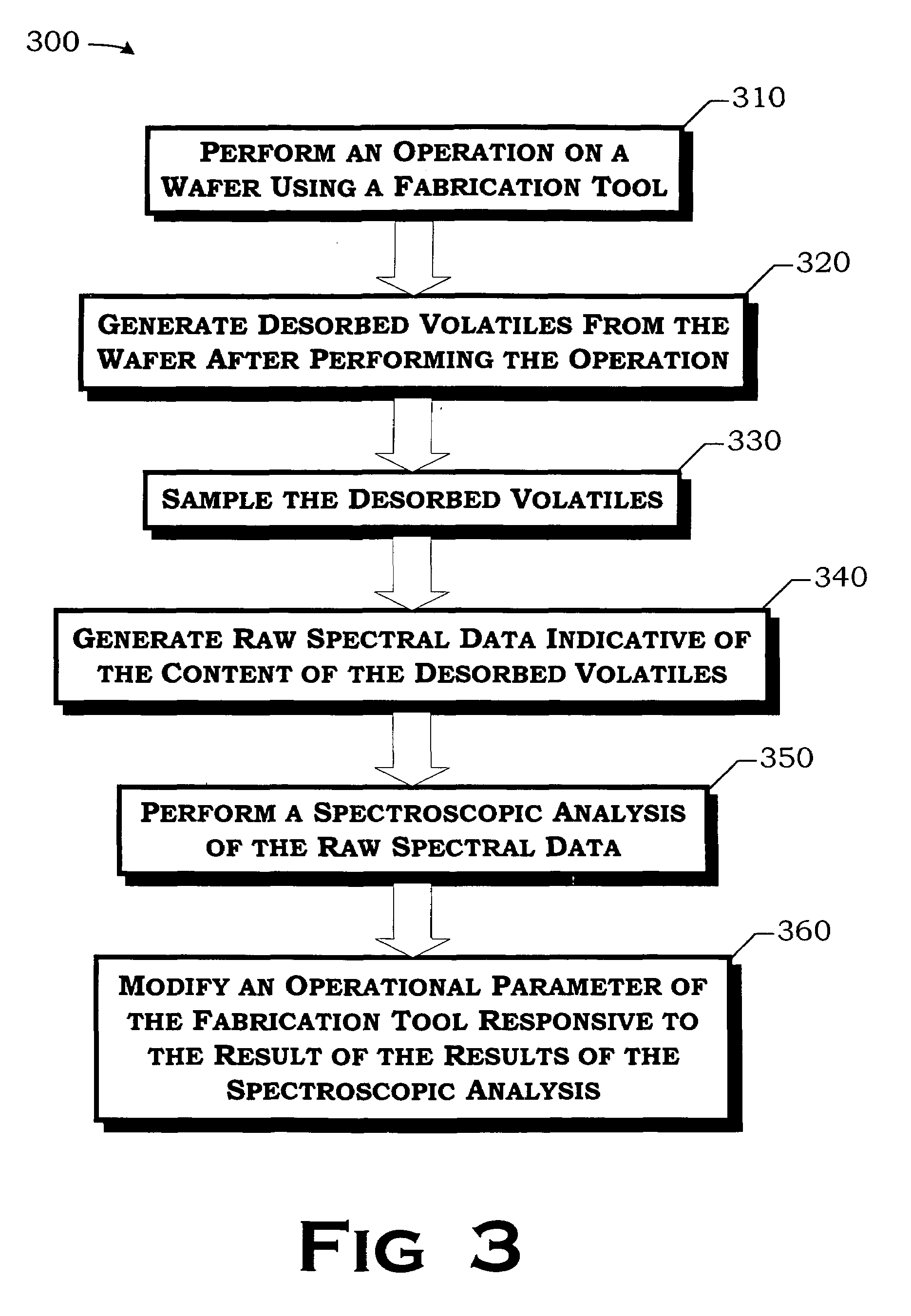
[0025]Turning now to the drawings, FIG. 1 illustrates one particular process flow 100 in accordance with the present invention. The process flow will typically comprise a portion of a much larger process flow for the fabrication of integrated circuits. FIG. 1 depicts operations only on a single w...


PUM

PropertyMeasurementUnit
Temperatureaaaaaaaaaa
Timeaaaaaaaaaa
Flow rateaaaaaaaaaa

Abstract

A technique for use in fabricating an integrated circuit are disclosed. The method generally begins by performing an operation on a wafer using a fabrication tool. Next, volatiles are desorbed from the wafer. The desorbed volatiles are sampled and raw spectral data indicating the content of the desorbed volatiles is generated. The raw spectral data is subjected to a spectroscopic analysis. An operational parameter of the fabrication tool is then modified responsive to the result of the results of the spectroscopic analysis. In one particular aspect of the invention, a controller receives the raw spectral data and processes the raw spectral data to determine the presence of a residual material on the wafer. The controller then controls the process flow operation to reduce the amount of the residual material on the wafer responsive to the results of processing the raw spectral data. Other aspects of the invention include the apparatus implementing the process flow and the controller itself.

Description

BACKGROUND OF THE INVENTION[0001]1. Field of the Invention[0002]The present invention relates to a method for controlling the presence and amount of residual material on a wafer prior to metal deposition in a semiconductor fabrication process and, more particularly, to a closed loop technique employing a residual gas analyzer for accomplishing the same.[0003]2. Description of the Related Art[0004]Integrated circuits are manufactured from wafers of a semiconducting substrate material. Layers of materials are added, removed, and / or treated during fabrication to create the integrated, electrical circuits that make up the device. Virtually any fabrication process essentially comprises the following four basic operations:[0005]layering, or adding thin layers of various materials to a wafer from which a semiconductor is produced;[0006]patterning / etching, or removing selected portions of the added layers;[0007]doping, or placing specific amounts of dopants in selected portions of the wafer...

Claims


Application Information

Patent Timeline
IPC IPC(8): H01L21/00C23C14/56C23C16/44H01L21/66
CPCC23C14/564C23C16/4401H01L22/20H01L2924/0002H01L2924/00
Inventor BRENNAN, WILLIAM S.
Owner TAIWAN SEMICON MFG CO LTD
Why Eureka
Try Eureka