Method for forming a semiconductor device

a semiconductor and film technology, applied in the field of semiconductor devices having a three-layer structure of metalinsulatorsemiconductor, can solve the problems of less complete high-k film, prone to the formation of conductive defects, and conventional amorphous high-k film has a problem in heat resistance, so as to improve the heat resistance of easy and reliably form metal-containing silicon oxide film, the effect of high level of amorphous metal-containing silicon oxid

Inactive Publication Date: 2005-10-18
TAIWAN SEMICON MFG CO LTD
View PDF10 Cites 15 Cited by
  • Summary
  • Abstract
  • Description
  • Claims
  • Application Information

AI Technical Summary

Benefits of technology

[0024]In this way, it is possible to easily and reliably form the metal-containing silicon oxide film. Moreover, the high level of amorphousness of the metal-containing silicon oxide film is maintained even at high temperatures, as that of a thermal oxide film, and thus the heat resistance of the metal-containing silicon oxide film is improved.
[0025]In a case where a thermal oxidation process is performed on a metal film, it is preferred that the thermal oxidation process is a rapid thermal oxidation process. Preferably, the rapid thermal oxidation process is performed in a pyrogenic atmosphere, in which case it is possible to further reduce the interface states occurring between the metal-containing silicon oxide film and the silicon layer and to further stabilize the composition of the metal-containing silicon oxide film. Moreover, if the rapid thermal oxidation process is performed by using infrared rays, it is possible to form the metal-containing silicon oxide film with a very small thickness.

Problems solved by technology

A high-k film is less complete than a thermal oxide film in terms of amorphousness (specifically, it is more easily turned into a polycrystalline state), and is more prone to the formation of conductive defects.
Moreover, a conventional amorphous high-k film has a problem in terms of heat resistance.
Specifically, while it is necessary for putting a high-k gate insulating film into practical use to perform various heat treatments such as an activation heat treatment after the conventional low-temperature formation of an amorphous high-k film, these heat treatments destroy the amorphous structure of the high-k film and turn it into a polycrystalline structure.
As a result, even if an amorphous high-k film immediately after deposition has a significantly suppressed leak current as compared with a thermal oxide film, the high-k film cannot continue to suppress the leak current therethrough after it is turned into a polycrystalline state through the subsequent high-temperature heat treatments, as described above.
Thus, the high-k film can no longer function as a gate insulating film.

Method used


Image

  • Method for forming a semiconductor device
  • Method for forming a semiconductor device
  • Method for forming a semiconductor device

Examples


first embodiment

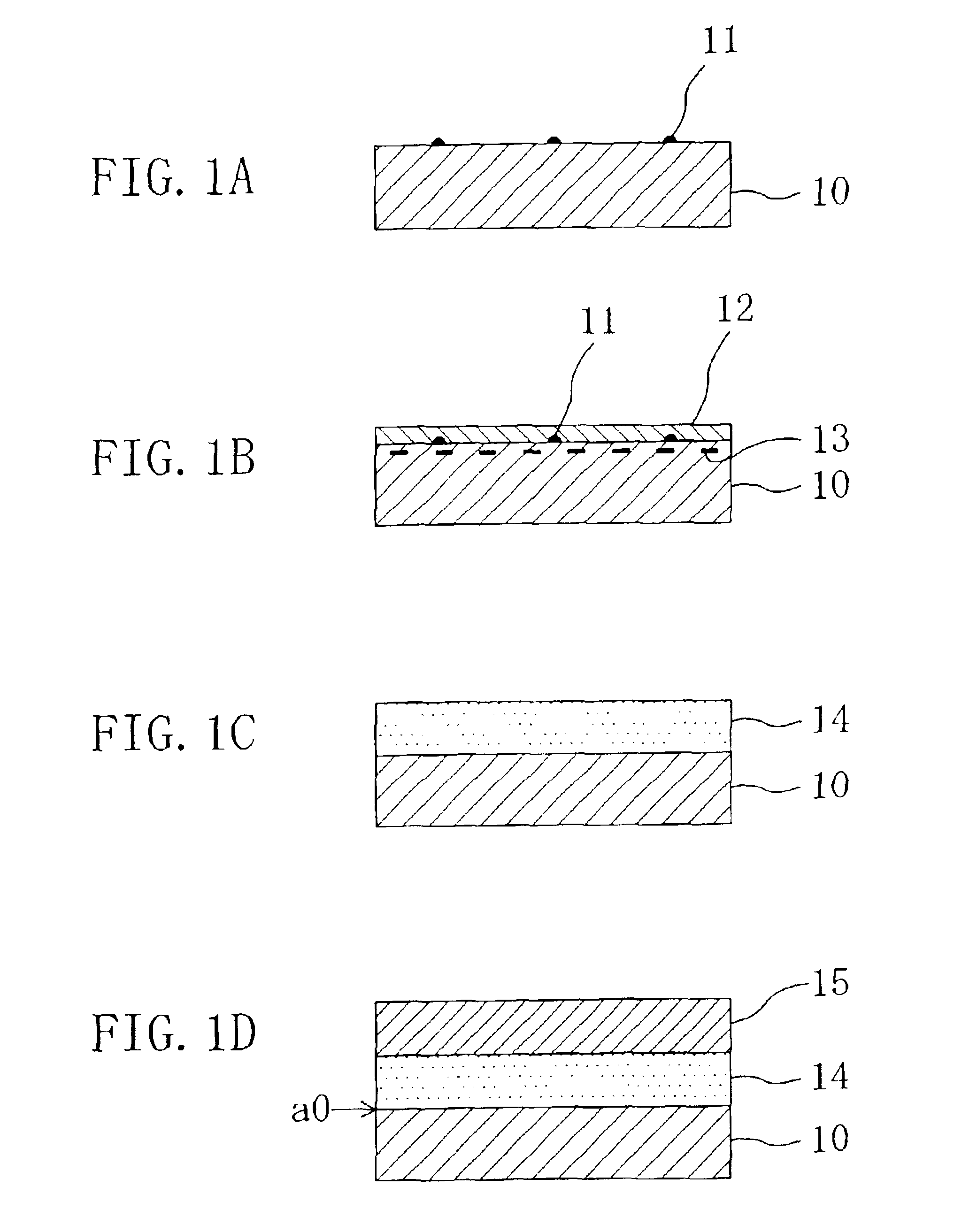
[0042]A semiconductor device, and a method for manufacturing the same, according to the first embodiment of the present invention will now be described with reference to the drawings for a MOSFET that uses a metal oxide as the insulator in a three-layer structure of metal-insulator-semiconductor.

[0043]FIG. 1A to FIG. 1D are cross-sectional views illustrating steps in the method for manufacturing a semiconductor device according to the first embodiment of the present invention. Note that steps such as the well formation, the isolation formation, the ion implantation for threshold control, and also the contact formation and the subsequent steps, will not be described below.

[0044]First, wet processes such as a pre-oxidation process, for example, are performed on the (001) surface of a silicon substrate 10, as illustrated in FIG. 1A. Specifically, cleaning with hot water, cleaning with buffered hydrogen fluoride into which a hydrogen peroxide solution is mixed, or cleaning with an impro...

second embodiment

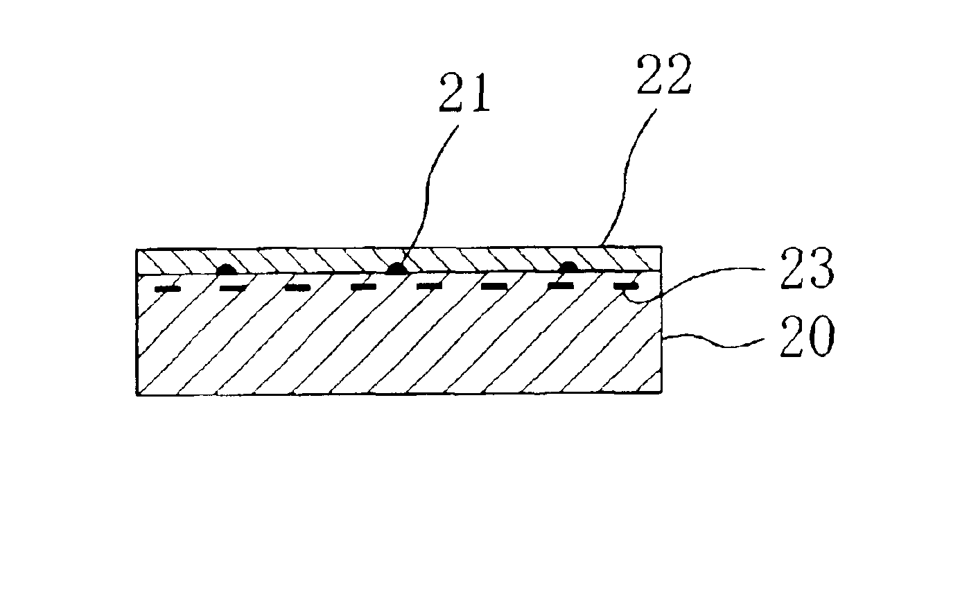
[0070]A semiconductor device, and a method for manufacturing the same, according to the second embodiment of the present invention will now be described with reference to the drawings for a MOSFET that uses a metal oxide as the insulator in a three-layer structure of metal-insulator-semiconductor.

[0071]FIG. 3A to FIG. 3D are cross-sectional views illustrating steps in the method for manufacturing a semiconductor device according to the second embodiment of the present invention. Note that steps such as the well formation, the isolation formation, the ion implantation for threshold control, and also the contact formation and the subsequent steps, will not be described below.

[0072]First, wet processes such as a pre-oxidation process, for example, are performed on the (001) surface of a silicon substrate 20, as illustrated in FIG. 3A. Specifically, cleaning with hot water, cleaning with buffered hydrogen fluoride into which a hydrogen peroxide solution is mixed, or cleaning with an imp...


PUM

PropertyMeasurementUnit
thicknessaaaaaaaaaa
thicknessaaaaaaaaaa
thicknessaaaaaaaaaa

Abstract

A metal film containing a metal is formed on a silicon layer, and then a surface portion of the silicon layer and the metal film are oxidized so as to form a silicon oxide film containing the metal in a surface portion of the silicon layer.

Description

BACKGROUND OF THE INVENTION[0001]The present invention relates to a semiconductor device having a three-layer structure of metal-insulator-semiconductor, and a method for manufacturing the same, and more particularly to a field effect transistor using a metal oxide film having a high dielectric constant as a gate insulating film material, and a method for manufacturing the same.[0002]A type of field effect transistor (hereinafter referred to as “FET”) used in the prior art is a MOSFET having a three-layer structure of metal-insulator-semiconductor. As MOSFETs are miniaturized at a significant rate, the thickness of a conventional gate oxide film has been reduced at an accelerated rate. The thickness of a gate oxide film is now as small as about 2 nm. However, when the physical thickness of a gate oxide film is reduced below about 2 nm, the transmittance of electrons through the gate oxide film increases dramatically, resulting in an excessive tunnel leak current flowing between the ...

Claims


Application Information

Patent Timeline
Patent Type & Authority Patents(United States)
IPC IPC(8): H01L21/28H01L29/40H01L21/02H01L29/51H01L27/04H01L21/316H01L21/822H01L29/78
CPCH01L21/28088H01L21/28176H01L21/28229H01L29/517
Inventor NIWA, MASAAKI
Owner TAIWAN SEMICON MFG CO LTD
Why Eureka
Try Eureka