Power grid and bump pattern with reduced inductance and resistance

a bump pattern and power grid technology, applied in the direction of semiconductor devices, electrical equipment, semiconductor/solid-state device details, etc., can solve the problems of ic designers reducing direct current (dc) and/or ac voltage variations at the transistor level of ic chips, and the design of ic chips becomes increasingly complicated. , to achieve the effect of reducing dc and/or ac voltage variations, low resistance and low inductan

Active Publication Date: 2005-11-01
ORACLE INT CORP
View PDF5 Cites 3 Cited by
  • Summary
  • Abstract
  • Description
  • Claims
  • Application Information

AI Technical Summary

Benefits of technology

[0007]The present invention provides novel methods and apparatus for reducing DC and/or AC voltage variations at the transistor level of IC chips, in part, by creating novel power and ground bump patterns and/or novel power and ground grids. In an embodiment, these patterns and grids may be located at the top metal layer of an IC, w

Problems solved by technology

As the functionality requirements of today's electronic products increase, the IC designs associated with these products also become increasingly more complicated.
As these designs become more compact, in part, to incorporate additional functionality in the same floor space, voltage variations at the transistor level quickly become a significant problem for designers.
More specifically, a challenging issue facing today's IC designers is reducing direct current (DC) and alternating current (AC) voltage variations at the transistors of IC chips.
Accordingly, problems associated with the

Method used


Image

  • Power grid and bump pattern with reduced inductance and resistance
  • Power grid and bump pattern with reduced inductance and resistance
  • Power grid and bump pattern with reduced inductance and resistance

Examples


Embodiment Construction

[0015]In the following description, numerous details are set forth. It will be apparent, however, to one skilled in the art that embodiments of the invention may be practiced without these specific details. In other instances, well-known structures, devices, and techniques have not been shown in detail, in order to avoid obscuring the understanding of the description. The description is thus to be regarded as illustrative instead of limiting.

[0016]Reference in the specification to “one embodiment” or “an embodiment” means that a particular feature, structure, or characteristic described in connection with the embodiment is included in at least an embodiment of the invention. The appearances of the phrase “in one embodiment” in various places in the specification are not necessarily all referring to the same embodiment.

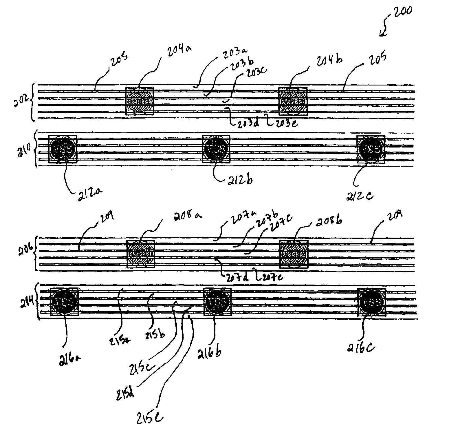
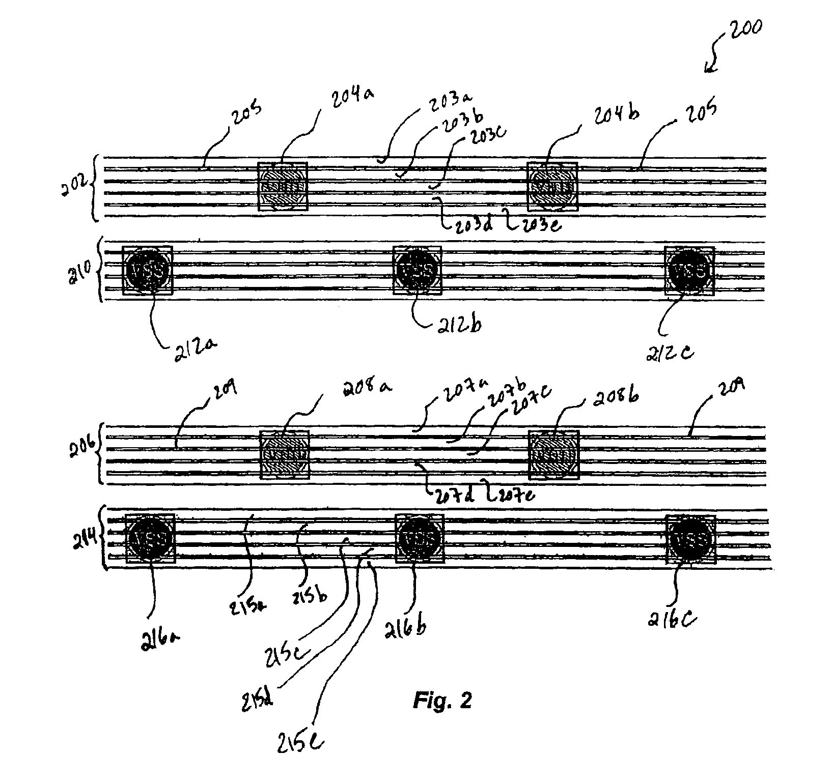
[0017]FIG. 2 illustrates an exemplarily cross-sectional view of a power grid 200 in accordance with an embodiment of the present invention. The power grid 200 includes...


PUM


Abstract

Disclosed are novel methods and apparatus for efficiently providing power buses and bump patterns with reduced inductance and/or resistance. In an embodiment, an apparatus is disclosed. The apparatus includes a plurality of power and ground bus pairs. Each power and ground bus pair may have a power bus and a ground bus. The apparatus further includes a first power bus from a first pair of the plurality of power and ground bus pairs. The first power bus may include a plurality of power bumps. The apparatus also includes a first ground bus from the first pair of the plurality of power and ground bus pairs. The first ground bus may include a plurality of ground bumps. Each of the plurality of power/ground bumps may be substantially equidistance from any immediately neighboring ground bump of the first ground bus.

Description

FIELD OF INVENTION[0001]The present invention generally relates to power distribution in integrated circuits (ICs). More specifically, an embodiment of the present invention relates to a low inductance and resistance power bus and bump pattern.BACKGROUND OF INVENTION[0002]As the functionality requirements of today's electronic products increase, the IC designs associated with these products also become increasingly more complicated. Examples of such IC designs include very large-scale integration (VLSI) circuits such as microprocessor chips (including those provided by Sun Microsystems, Inc., of Palo Alto, Calif.). As these designs become more compact, in part, to incorporate additional functionality in the same floor space, voltage variations at the transistor level quickly become a significant problem for designers. More specifically, a challenging issue facing today's IC designers is reducing direct current (DC) and alternating current (AC) voltage variations at the transistors o...

Claims


Application Information

Patent Timeline
IPC IPC(8): H01L23/48H01L23/50H01L23/52H01L23/528H01L21/82H01L21/822H01L27/04
CPCH01L23/50H01L23/528H01L2924/0002H01L2924/00
Inventor TOMSIO, NAYONSCHMIDT, STEVEN A.WHITNEY, LINDA S.
Owner ORACLE INT CORP
Why Eureka
Try Eureka