LED power package

a power package and led technology, applied in the field of lighting arts, can solve the problems of low luminous output of leds for lighting applications, complex packaging, and limiting factors of luminous outpu

Inactive Publication Date: 2005-11-15
PROLIGHT OPTO TECH
View PDF20 Cites 244 Cited by
  • Summary
  • Abstract
  • Description
  • Claims
  • Application Information

AI Technical Summary

Benefits of technology

[0009]In accordance with another aspect, a light emitting diode (LED) package is disclosed. An LED has a first side on which a pair of electrical contacts are arranged and a second side. A submount has a first side onto which the first side of the LED is bonded and a second side. Said submount provides: a plurality of electrically conductive paths that extend from the second side of the submount to the first s...

Problems solved by technology

However, GaN-based power LEDs for lighting applications suffer from low luminous output.
Heat dissipation is a limiting factor in the luminous output and reliability of power LEDs.
Packaging is complex due to the separate steps of bonding the GaN layers to the sub-mount, bonding the sub-mount to the associated support, and wire-bonding the bonding pads to the lead frame.
The package is incompatible with wafer-le...

Method used


Image

  • LED power package
  • LED power package
  • LED power package

Examples


Embodiment Construction

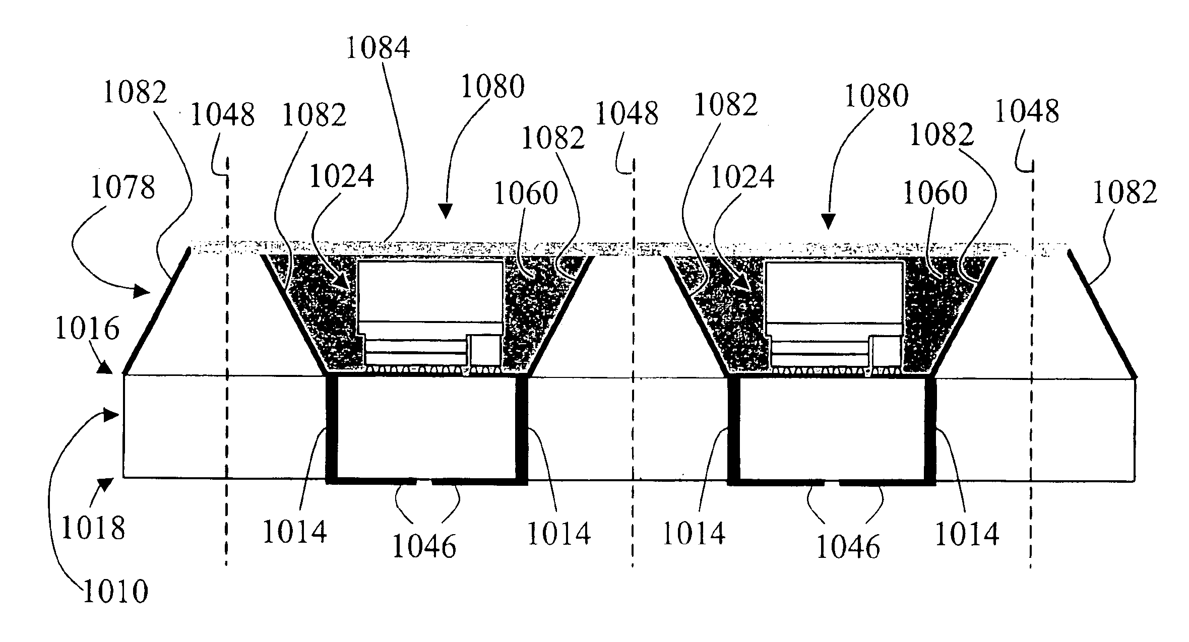
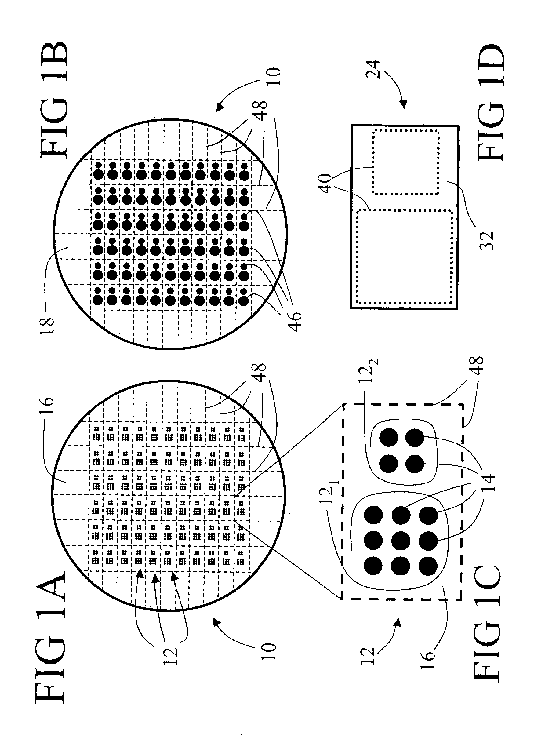
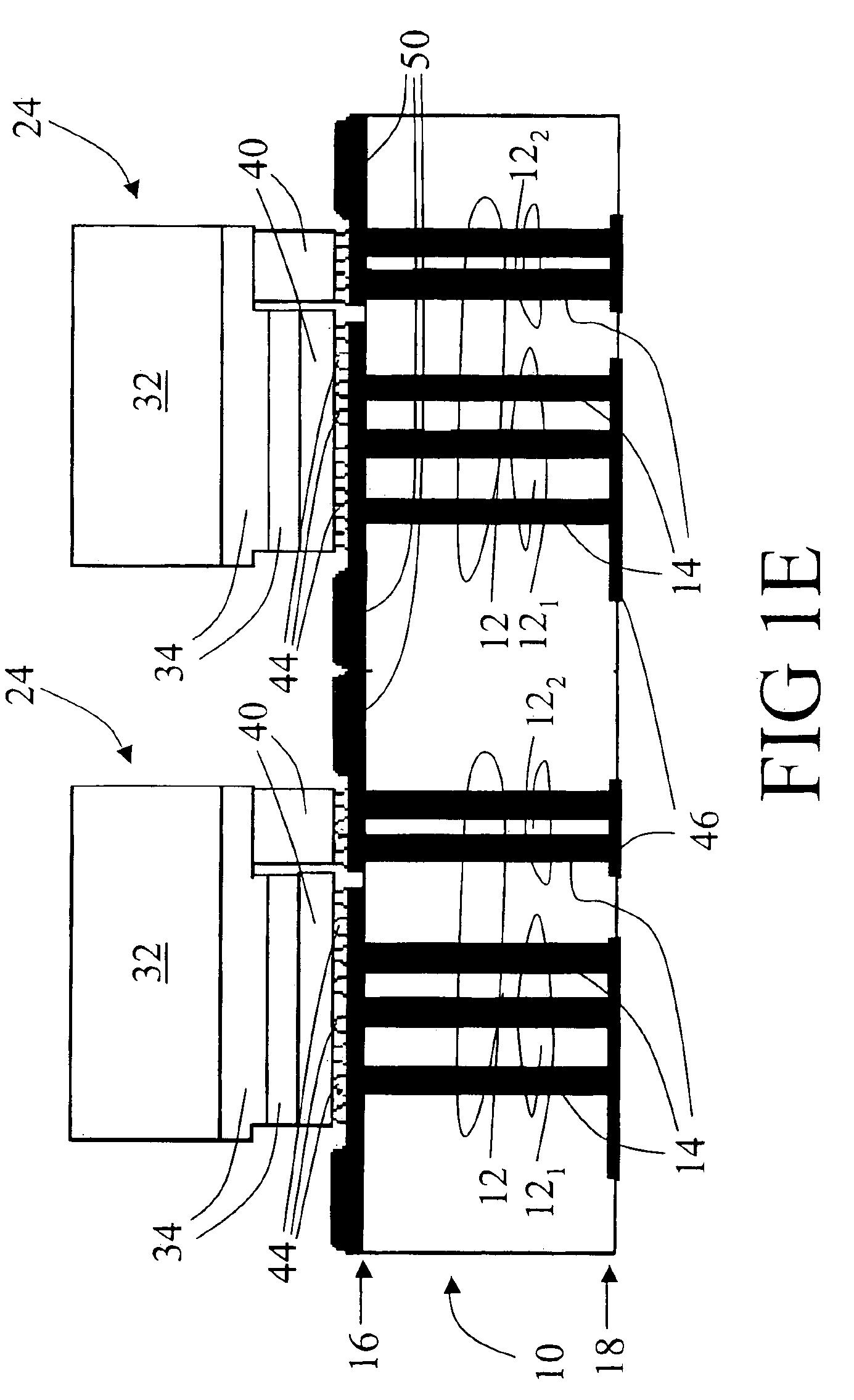
[0032]With reference to FIGS. 1A-1E, a plurality of surface mount light emitting diode (LED) packages are produced using a common sub-mount wafer 10 that includes arrays 12 of electrically conductive vias 14 that pass from a frontside 16 of the sub-mount wafer 10 to a backside 18 of the sub-mount wafer 10.

[0033]LED dice 24 each include a light transmissive substrate 32 on which p-type and n-type semiconductor layers 34 are deposited to form a light emitting p / n diode structure that emits light when electrically energized. Metallic, polymeric, or another type of p-type and n-type electrodes 40 of are formed on the semiconductor layers 34 for electrically energizing the LED die 24. In one preferred embodiment, the LED dice 24 are GaN-based LEDs in which the semiconductor layers 34 are a multiple layer stack of AlN, GaN, InN, or alloys thereof which are deposited on a light-transmissive sapphire or SiC substrate. Although two semiconductor layers 34 are shown, it should be appreciated ...


PUM


Abstract

Surface mount light emitting diode (LED) packages each contain a light emitting diode (LED) die (24). A plurality of arrays of openings are drilled into an electrically insulating sub-mount wafer (10). A metal is applied to the drilled openings to produce a plurality of via arrays (12). The LED dice (24) are flip-chip bonded onto a frontside (16) of the sub-mount wafer (10). The p-type and n-type contacts of each flip-chip bonded LED (24) electrically communicate with a solderable backside (18) of the sub-mount wafer (10) through a via array (12). A thermal conduction path (10, 12) is provided for thermally conducting heat from the flip-chip bonded LED dice (24) to the solderable backside (18) of the sub-mount wafer (10). Subsequent to the flip-chip bonding, the sub-mount wafer (10) is separated to produce the surface mount LED packages.

Description

[0001]This application in a divisional of Ser. No. 10 / 402,505 filed on Mar. 28, 2003.BACKGROUND OF THE INVENTION[0002]The present invention relates to the lighting arts. It is particularly applicable to the fabrication of high-brightness gallium nitride (GaN) based light emitting diodes (LEDs) and LED arrays, and will be described with particular reference thereto. However, the invention also finds application in connection with other types of LEDs and in other LED applications.[0003]LEDs, particularly those fabricated from gallium nitride (GaN), aluminum nitride (AlN), indium nitride (InN), and various alloys and layer combinations thereof, are suitable for illumination applications in the ultraviolet and blue wavelength ranges. Additionally, GaN-based LEDs which are coated with a wavelength-converting phosphor are suitable for producing white or selectably colored light for illumination. Such LEDs have a number of advantages over other types of illuminators, including compactness,...

Claims


Application Information

Patent Timeline
IPC IPC(8): H01L21/00H01L31/02H01L33/00H01L33/48H01L33/62
CPCH01L24/97H01L33/486H01L33/62H01L2224/16H01L2224/97H01L2924/01013H01L2924/01029H01L2924/01033H01L2924/01046H01L2924/01047H01L2924/01049H01L2924/01078H01L2924/01079H01L2924/01082H01L2924/3011H01L2224/81H01L2924/01006H01L2924/01023H01L2924/01074H01L2924/12041H01L2924/12042H01L33/647H01L2224/05568H01L2224/05023H01L2224/05001H01L2924/00014H01L24/05H01L24/16H01L2224/0603H01L2224/06051H01L2924/00H01L2224/05599H01L2224/05644H01L2224/05155H01L2224/05166
Inventor CHEN, CHEN-LUN HSINGWEAVER, JR., STANTONELIASHEVICH, IVANLIBON, SEBASTIENARIK, MEHMETSHADDOCK, DAVID
Owner PROLIGHT OPTO TECH
Why Eureka
Try Eureka