Circuitized substrates utilizing three smooth-sided conductive layers as part thereof, method of making same, and electrical assemblies and information handling systems utilizing same

a technology of conductive layer and circuitized substrate, which is applied in the direction of insulating substrate metal adhesion improvement, printed circuit aspects, and association of printed circuit non-printed electric components, etc., can solve the problems of adversely affecting signal passage, signal deterioration, and high-speed connection subject to various detrimental effects, so as to enhance the circuitized substrate art

Inactive Publication Date: 2005-11-15
I3 ELECTRONICS +1
View PDF12 Cites 19 Cited by
  • Summary
  • Abstract
  • Description
  • Claims
  • Application Information

AI Technical Summary

Benefits of technology

[0022]It is, therefore, a primary object of the present invention to enhance the circuitized substrate art by providing a circuitized substrate having the advantageous features taught herein.
[0023]It is another object of the invention to provide a method of making such a circuitized substrate which can be accomplished in a relatively facile manner and at relatively low costs.
[0026]According to one aspect of the invention, there is provided a method of making a circuitized substrate comprising providing a first electrically conductive layer with first and second opposing smooth sides, providing second and third electrically conductive layers each having a first smooth side and a second opposing side of a roughness greater than that of the first smooth sides of the second and third electrically conductive layers, treating the three electrically conductive layers with a chemical treatment so as to minimally increase the roughness of the first and second smooth sides of the first electrically conductive layer and the first smooth sides of the second and third electrically conductive layers, providing first and second dielectric layers, bonding the first and second dielectric layers to the first and second opposing smooth sides of the first electrically conductive layer, respectively, after the treating of the first electrically conductive layer with the chemical treatment, bonding the first smooth sides of both second and third electrically conductive layers to the first and second dielectric layers, respectively, after treating of the first smooth sides of the second and third electrically conductive layers with the chemical treatment, and forming a circuit pattern within at least one of the second and third electrically conductive layers.

Problems solved by technology

Such high-speed connections are subjected to various detrimental effects, e.g., signal deterioration (also referred to as signal attenuation), caused by the inherent characteristics of such known substrate circuitry wiring.
Unfortunately, such roughness may also adversely affect signal passage if too excessive.
Unfortunately, if the foil is too thin, it may be damaged, e.g., severed or torn in sections, from the relatively high stresses exerted on the copper foil during this processing.
However, such processes are typically expensive to operate, often requiring relatively expensive equipment, costly chemical baths, as well as prolonged periods during which the foil is so treated, thereby extending the total time of manufacture of the end product.
Moreover, depressed parts are not polished, so that the amount of copper lost by the polishing steps is extremely minute.

Method used


Image

  • Circuitized substrates utilizing three smooth-sided conductive layers as part thereof, method of making same, and electrical assemblies and information handling systems utilizing same
  • Circuitized substrates utilizing three smooth-sided conductive layers as part thereof, method of making same, and electrical assemblies and information handling systems utilizing same
  • Circuitized substrates utilizing three smooth-sided conductive layers as part thereof, method of making same, and electrical assemblies and information handling systems utilizing same

Examples


Embodiment Construction

[0035]For a better understanding of the present invention, together with other and further objects, advantages and capabilities thereof, reference is made to the following disclosure and appended claims in connection with the above-described drawings. Like figure numbers will be used from FIG. to FIG. to identify like elements in these drawings.

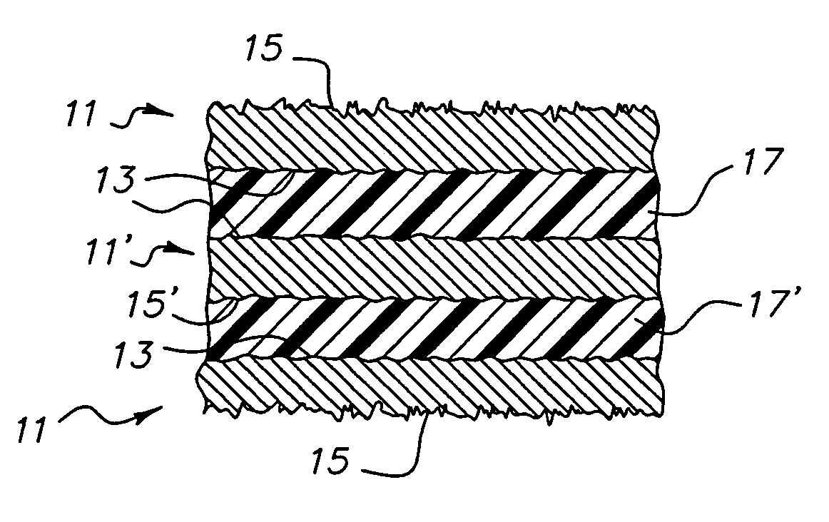
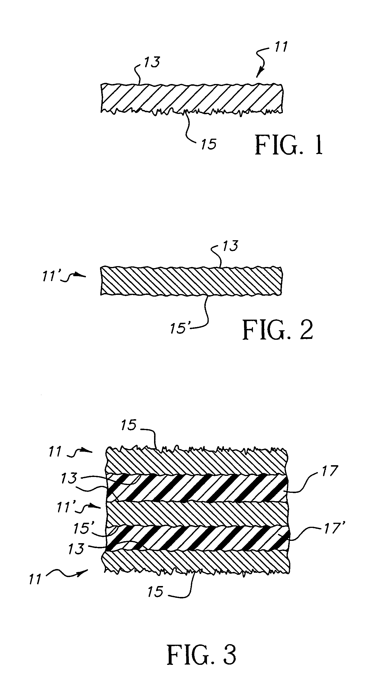
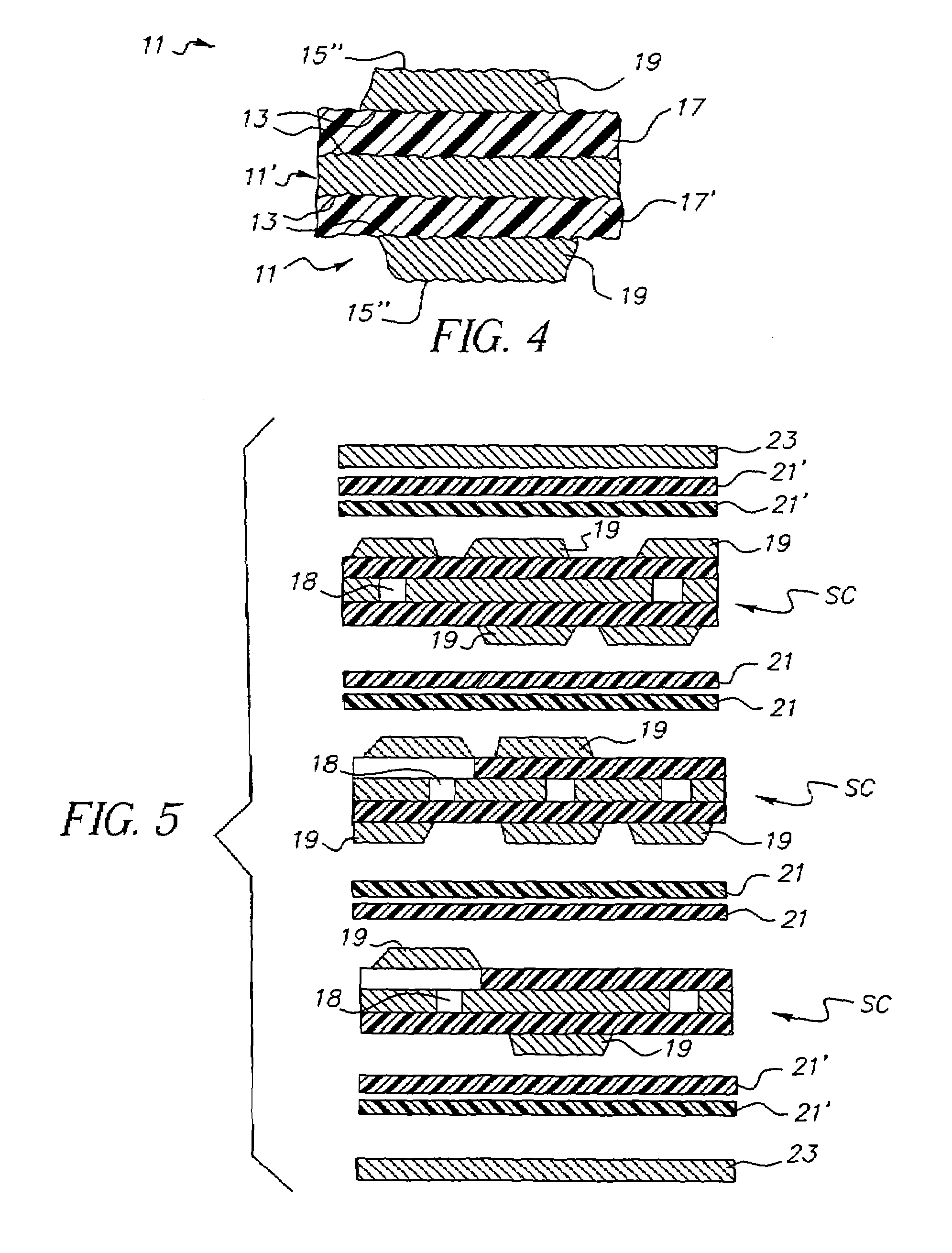
[0036]By the term “circuitized substrate” as used herein is meant to include substrates having at least two dielectric layers and at least three metallurgical conductive layers. Examples include structures made of dielectric materials such as fiberglass-reinforced epoxy resins (some referred to as “FR-4” dielectric materials in the art), polytetrafluoroethylene (Teflon), polyimides, polyamides, cyanate resins, polyphenylene ether resins, photoimageable materials, and other like materials wherein the conductive layers are each a metal layer (e.g., power, signal and / or ground) comprised of suitable metallurgical materials such as copper (prefer...


PUM


Abstract

A circuitized substrate in which three conductive layers (e.g., electroplated copper foil) are bonded (e.g., laminated) to two dielectric layers. Each of the foil surfaces which physically bond to a respective dielectric layer are smooth (e.g., preferably by chemical processing) and may include a thin, organic layer thereon. One of the conductive layers may function as a ground or voltage (power) plane while the other two may function as signal planes with a plurality of individual signal lines as part thereof. An electrical assembly and an information handling system utilizing such a circuitized substrate are also provided, as is a method of making the substrate.

Description

TECHNICAL FIELD[0001]The invention relates to circuitized substrates utilizing conductive sheets as part thereof, methods for making such substrates, and to electrical assemblies and information handling systems utilizing such substrates. One primary example of such a circuitized substrate is a printed circuit (or wiring) board (or card) and another is a chip carrier substrate, both of which are produced by the assignee of the present invention.CROSS REFERENCE TO CO-PENDING APPLICATION[0002]In Ser. No. 10 / 354,000, entitled “High Speed Circuit Board And Method For Fabrication” (inventors B. Chan et al), there is defined a multilayered circuitized substrate including two multilayered portions, one of these able to electrically connect electronic components mounted on the substrate to assure high frequency connections there-between. The substrate may further include a “conventional” substrate portion of known materials so as to reduce costs while assuring a structure having an overall ...

Claims


Application Information

Patent Timeline
Patent Type & Authority Patents(United States)
IPC IPC(8): H01L21/02H01L21/44H05K3/38H05K3/46
CPCH05K3/383H05K3/4641H05K2201/0355H05K2203/0353H01L2224/16225H01L2224/73253H01L2924/15311H01L2924/0002H01L2924/00
Inventor CHAN, BENSONLAUFFER, JOHN M.
Owner I3 ELECTRONICS
Why Eureka
Try Eureka