Capacitor in semiconductor device having dual dielectric film structure and method for fabricating the same

a semiconductor device and dielectric film technology, applied in the direction of fixed capacitor details, fixed capacitors, coatings, etc., can solve the problems of oxidation film not being lowered, dielectric properties deteriorating and damaged, and the integration process which follows the wiring process is not good, so as to achieve the effect of suppressing the occurrence of leakage current and increasing the charging capacity of capacitors

Inactive Publication Date: 2005-11-15
SK HYNIX INC
View PDF6 Cites 0 Cited by
  • Summary
  • Abstract
  • Description
  • Claims
  • Application Information

AI Technical Summary

Benefits of technology

[0025]Accordingly, the present invention has been made to solve the above-mentioned problems occurring in the prior art, and an object of the present invention is to provide a capacitor in a semiconductor device with a dual dielectric film structure, which is capable of providing larger charging capacity for a capacitor than a conventional dielectric material by employing a dual dielectric film composed of a Ta2O5 / Si3N4 thin film structure, and can effectively suppress the occurrence of leakage current, thereby being suitable for a highly integrated semiconductor device, and a fabrication method therefor.

Problems solved by technology

Meanwhile, a depth of focus is not assured in the following exposure process due to the differences of height produced between a cell region and a peripheral circuit region when the height of the capacitor increases, which results in a bad effect upon the integration process which follows the wiring process.
However, according to the above-noted prior art, vacancy atoms Ta arising from the differences of the composition ratio between Tantalum (Ta) and Oxygen (O) exist in the thin film, because the Ta2O5 thin film has an unstable stoichiometry.
As a result, leakage current increases due to carbon atoms, ions and radicals that exist as impurities in the Ta2O5 thin film, and the dielectric properties become deteriorated and damaged.
Therefore, the thickness of the oxidation film can not be lowered to below 30 Å, resulting in limitations in achieving a large charging capacity for a capacitor.

Method used


Image

  • Capacitor in semiconductor device having dual dielectric film structure and method for fabricating the same
  • Capacitor in semiconductor device having dual dielectric film structure and method for fabricating the same
  • Capacitor in semiconductor device having dual dielectric film structure and method for fabricating the same

Examples


Embodiment Construction

[0031]Hereinafter, a preferred embodiment of the present invention will be described with reference to the accompanying drawings.

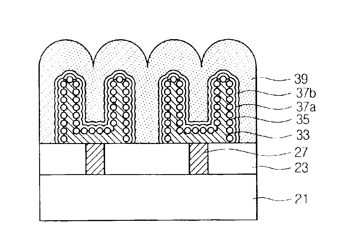
[0032]FIGS. 2A to 2D are sectional views illustrating each step in a method for fabricating a capacitor in a semiconductor device having a dual dielectric film structure in accordance with the present invention.

[0033]In accordance with one embodiment of the present invention, as shown in FIG. 2A, a first interlayer insulating film 23 is first deposited on a semiconductor substrate 21, and then photo-sensitive materials are distributed thereon and a first photo-mask (not shown) for making a plug contact is formed by carrying out an exposure process and a developing process using photolithography technology and selective patterning of photo-sensitive materials.

[0034]Next, a plug contact hole 25, which exposes a portion of the semiconductor substrate 21, is formed by patterning of the first interlayer insulating film 23 using the first photo-mask (not shown) ...


PUM

PropertyMeasurementUnit
temperatureaaaaaaaaaa
pressureaaaaaaaaaa
temperatureaaaaaaaaaa

Abstract

A capacitor in a semiconductor device having a dual dielectric film structure and a fabrication method therefor are disclosed. The capacitor comprises: a lower electrode formed on a semiconductor substrate, a dielectric film of a dual dielectric film structure composed of an Si3N4 chloride-free thin film and a Ta2O5 thin film, which is formed on the lower electrode, and an upper electrode formed on the dielectric film. Meanwhile, the method for fabricating the capacitor comprises the steps of: forming a lower electrode on a semiconductor substrate, forming a dielectric film of a dual dielectric film structure composed of an Si3N4 thin film and a Ta2O5 thin film on the lower electrode, and forming an upper electrode on the dielectric film.

Description

BACKGROUND OF THE INVENTION[0001]1. Field of the Invention[0002]The present invention relates to a method for fabricating a capacitor in a semiconductor device, and more particularly to a method for fabricating a capacitor in a semiconductor device having a dual dielectric film structure composed of Ta2O5 / Si3N4, and a capacitor fabricated thereby.[0003]2. Description of the Prior Art[0004]Recently, as high integration of memory products has become accelerated following the development of microscopic fabrication process technologies for semiconductors, unit cell area is largely decreased and driving voltage has been lowered considerably.[0005]However, the necessary capacity of the capacitor for the driving of memory elements is required to increase above 25 fF per cell so as to suppress the contraction of the refresh time and to prevent the occurrence of soft errors, despite the reduction of the cell area.[0006]Accordingly, recently a three dimensional type electrical charge storage ...

Claims


Application Information

Patent Timeline
Patent Type & Authority Patents(United States)
IPC IPC(8): H01L21/02H01L21/314H01L21/318H01L21/316H01L21/8242H01L27/108
CPCH01L21/3143H01L21/31604H01L21/3185H01L28/40H01L28/84H01L28/90H01L21/02183H01L21/0217H01L21/022H01L21/02271H01L21/02219H01L21/0228H01L21/02356H10B99/00H01L21/02337
Inventor LEE, KEE JEUNGHONG, BYUNG SEOP
Owner SK HYNIX INC
Why Eureka
Try Eureka