Semiconductor device of chip-on-chip structure

Inactive Publication Date: 2005-11-15
ROHM CO LTD
View PDF23 Cites 65 Cited by
  • Summary
  • Abstract
  • Description
  • Claims
  • Application Information

AI Technical Summary

Benefits of technology

[0011]It is an object of the present invention to provide a semiconductor device which has a construction that a

Problems solved by technology

Improper positioning often makes it impossible to bond the corresponding bumps of the two semiconductor chips to each other.
However, there is a possibility that misalignment of th

Method used


Image

  • Semiconductor device of chip-on-chip structure
  • Semiconductor device of chip-on-chip structure
  • Semiconductor device of chip-on-chip structure

Examples


first embodiment

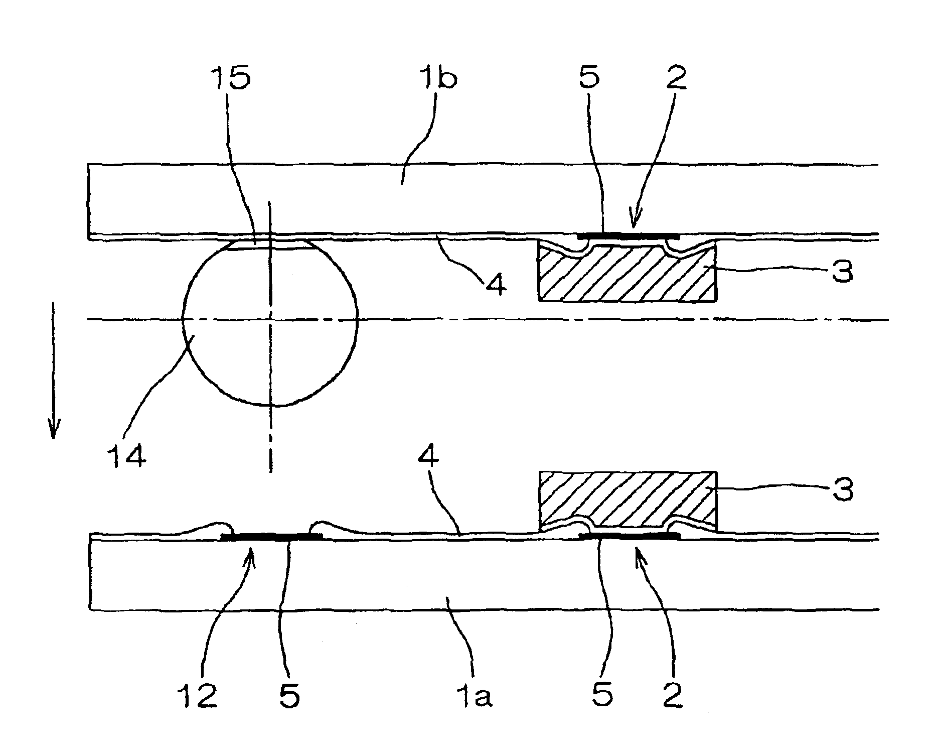
[0046]FIG. 1 is a diagram for explaining the construction of a semiconductor device according to the present invention, and illustrates sections of semiconductor chips 1a, 1b to be stacked. One 1a of the semiconductor chips has a pad 12 (an exposed portion of an internal interconnection 5) provided at a predetermined position in a peripheral portion thereof surrounding a device formation region on an active surface side thereof, for example, in a scribe line region thereof. The pad 12 functions as a registration recess. A bump 3 for ordinary electrical connection is provided on a pad 2 (an exposed portion of an internal interconnection 5) in the device formation region of the semiconductor chip 1b.

[0047]The other semiconductor chip 1b has a bump 3 provided on a pad 2 in a device formation region on an active surface side thereof, and a metal ball 14 bonded to a surface portion thereof corresponding to the position of the pad 12 of the semiconductor chip 1a. The metal ball 14 functi...

second embodiment

[0061]FIG. 5 is a sectional view illustrating the construction of a semiconductor device according to the invention, in which a bump provided on one of a pair of semiconductor chips to be stacked has a greater plan area than a corresponding bump provided on the other semiconductor chip. In FIG. 5, components corresponding to those illustrated in FIG. 1 are denoted by the same reference characters as in FIG. 1. However, it is not intended that the components denoted by the same reference character necessarily have an identical construction and function.

[0062]A bump 3a is provided in a device formation region on an active surface side of one 1a of the semiconductor chips 1a, 1b to be stacked. A bump 3b is provided in a device formation region on an active surface side of the other semiconductor chip 1b. In FIG. 5, the semiconductor chips 1a, 1b are to be stacked with a positional offset D.

[0063]The bump 3b has a standard mating surface area as in an ordinary design, but the bump 3a ha...

third embodiment

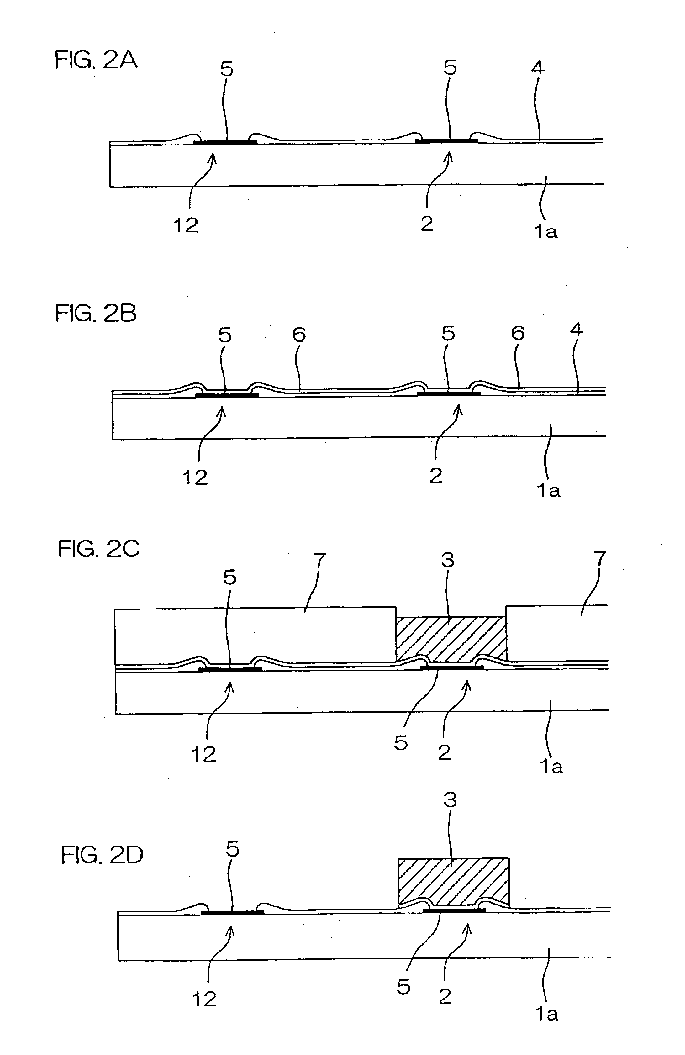
[0066]FIG. 7A is a perspective view illustrating a major portion of a semiconductor chip 21 according to the invention. Bumps 23 are provided on a device formation surface of the semiconductor chip 21, and a groove 22 is formed in a predetermined position within a peripheral portion, i.e., a scribe line region of the semiconductor chip 21. The formation of the groove may be achieved by etching a semiconductor substrate of the chip or by cutting the semiconductor substrate by a cutting tool.

[0067]Metal balls 24 are disposed in the groove 22 (see FIG. 7B). The metal balls 24 are composed of a soft metal such as solder, Au or Sn. One possible method for placement of the metal balls 24 is such that an operator places the metal balls 24 one by one in the groove 22 by means of tweezers by observation through a microscope but, a more practical method is such that the metal balls are introduced into the groove 22 by a guide.

[0068]FIG. 8A is a sectional view illustrating a state before anoth...


PUM


Abstract

A semiconductor device including a first semiconductor chip, a second semiconductor chip bonded to the first semiconductor chip in a stacked relation, and a registration structure which causes the first and second semiconductor chips to be positioned with respect to each other by depression-projection engagement therebetween. The registration structure includes, for example, a registration recess provided on a surface of the first semiconductor chip, and a registration projection provided on a surface of the second semiconductor chip for engagement with the registration recess. The registration projection may be a spherical member provided on the surface of the second semiconductor chip.

Description

[0001]This is a continuation of U.S. Ser. No. 09 / 511,105 filed Feb. 23, 2000, which is now abandoned.BACKGROUND OF THE INVENTION[0002]1. Field of the Invention[0003]The present invention relates to semiconductor devices of chip-on-chip structure. The invention further relates to a semiconductor chip to be bonded to a surface of a solid body (e.g., semiconductor chip or wiring board). The invention still further relates to an assembling process for a semiconductor device of chip-on-chip structure.[0004]2. Description of Related Art[0005]For substantial increase in integration level, attention has been directed to semiconductor devices of chip-on-chip structure in which semiconductor chips are arranged in a double-stacked relation.[0006]In such a semiconductor device, more specifically, the semiconductor chips to be stacked each have pad openings formed in a device formation surface thereof to partly expose internal interconnections. Electrode projections called “bumps” are respective...

Claims


Application Information

Patent Timeline
IPC IPC(8): H01L23/34H01L21/60H01L23/48H01L21/70H01L23/28H01L23/36H01L21/02H01L23/31H01L23/498H01L21/98H01L25/065H01L21/56H01L23/485H01L29/06
CPCH01L23/3128H01L23/36H01L23/49816H01L24/11H01L24/73H01L24/81H01L25/0657H01L25/50H01L24/13H01L21/563H01L29/0657H01L2224/0401H01L2224/0603H01L2224/1147H01L2224/13099H01L2224/1403H01L2224/16145H01L2224/81136H01L2224/81801H01L2225/06513H01L2225/06593H01L2924/01013H01L2924/01029H01L2924/01032H01L2924/01046H01L2924/01047H01L2924/01077H01L2924/01078H01L2924/01079H01L2924/10329H01L2924/3511H01L2924/01023H01L2924/01033H01L2924/0105H01L2924/014H01L2224/131H01L2224/13144H01L2924/00014H01L2224/13111H01L2924/0001H01L2224/10135H01L2224/10165H01L2224/14517H01L2224/81139H01L2224/81141H01L2224/11334H01L2224/17517H01L2224/05124H01L2224/05166H01L2224/05624H01L2224/05644H01L2224/05647H01L2224/05666H01L2224/05669H01L2224/141H01L2224/14051H01L24/16H01L2924/01074H01L2924/013
Inventor HIKITA, JUNICHINAKAGAWA, YOSHIKAZUYAMAMOTO, KOJI
Owner ROHM CO LTD
Why Eureka
Try Eureka