Method of manufacture of active matrix addressed polymer LED display

a technology of active matrix and polymer led display, which is applied in the field of information display using organic electroluminescent materials and thin film field effect transistors, can solve the problems of large cost advantages associated with fabricating polymer leds on flexible plastic substrates with roll-to-roll equipment, and the cost of such displays is also a significant factor in the overall price of portable computers using the sam

Inactive Publication Date: 2005-11-15
INNOLUX CORP
View PDF21 Cites 60 Cited by
  • Summary
  • Abstract
  • Description
  • Claims
  • Application Information

AI Technical Summary

Benefits of technology

[0009]It is a further object of the present invention to provide an OLED-based active matr...

Problems solved by technology

Active matrix liquid crystal displays for computers and the like provide significantly improved performance; however, the cost of such displays is also a significant factor in the overall price of portable computers using the same.
In addition, active matrix displays require substantially more power than passive displays since this type of display utilizes backlighting.
While OLEDs have the potential for reducing display cost...

Method used


Image

  • Method of manufacture of active matrix addressed polymer LED display
  • Method of manufacture of active matrix addressed polymer LED display
  • Method of manufacture of active matrix addressed polymer LED display

Examples


Embodiment Construction

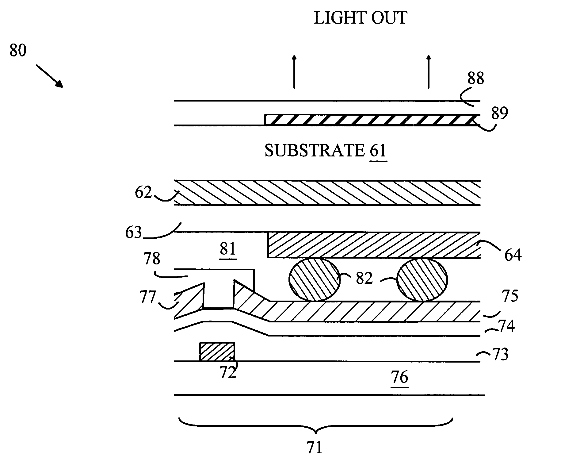
[0017]The present invention overcomes the problems associated with the above described prior art methods by utilizing a laminating technique that allows an OLED-based sheet of light emitting diodes formed on a flexible plastic substrate to be laminated onto a solid TFT substrate. In this manner, the cost advantages associated with OLEDs are preserved.

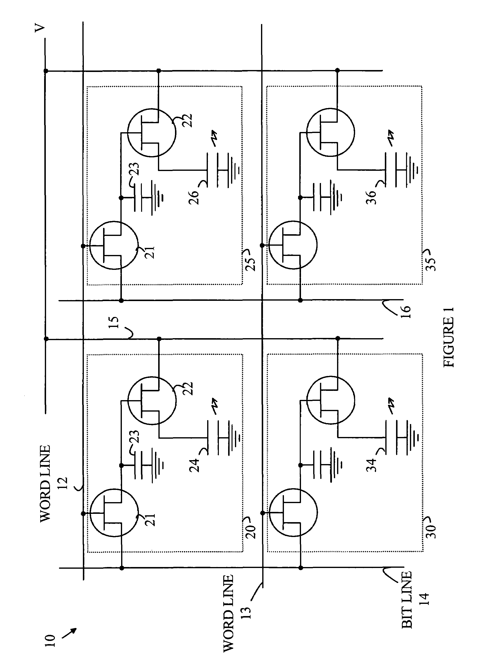
[0018]Refer now to FIG. 1 which is a schematic drawing of a portion of a display 10 according to the present invention. The portion of display 10 shown in FIG. 1 consists of four pixels 20, 25, 30, and 35. Each pixel consists of two TFT transistors, an OLED, and a capacitor for storing the intensity to be displayed by the OLED. The corresponding OLEDs are shown at 24, 26, 34, and 36. Referring to pixel 20, the current flowing through OLED 24 is determined by the voltage on the gate of TFT 22 and the supply voltage provided on bus 15. The voltage on the gate of TFT 22 is set by applying the desired voltage to a bit line 14 while placing ...


PUM


Abstract

A display having a plurality of light emitting pixels. Each pixels includes an isolation transistor, a driving circuit, and an organic light emitting diode (OLED). The driving circuit storing a value that determines the magnitude of the light emitted by that pixels, the driving circuit placing the OLED in a conducting path between the first and second power terminals. The driving circuit is programmed through the isolation transistor. In one embodiment of the present invention, the driving circuit includes a storage capacitor and a driving transistor. The OLEDs are part of an array of OLEDs. The array of OLEDs is constructed on a flexible sheet having first and second surfaces, the flexible sheet being transparent to light of a first wavelength. A transparent first electrode layer is in contact with the first surface. A light emitting layer including an organic polymer is in contact with the first electrode layer. A plurality of second electrodes, one such second electrode corresponding to each of the OLEDs, is in contact with the light emitting layer. Each second electrode has an isolated conducting area. The driving transistor are part of a transistor array having a plurality of connection points disposed on a surface, each connection point corresponding to one of the second electrodes in the array of OLEDs. The connection points are arranged such that each second electrode overlies the corresponding connection point when the array of OLEDs is properly aligned with the transistor array. The connection points are bonded to the corresponding second electrodes by a bonding layer.

Description

FIELD OF THE INVENTION[0001]The present invention relates to display devices, and more particularly, to information displays using organic electroluminescent materials and thin film field effect transistors.BACKGROUND OF THE INVENTION[0002]Active matrix liquid crystal displays for computers and the like provide significantly improved performance; however, the cost of such displays is also a significant factor in the overall price of portable computers using the same. In addition, active matrix displays require substantially more power than passive displays since this type of display utilizes backlighting.[0003]An active matrix liquid crystal display is constructed from two components that are separately constructed and then bonded together. The first component consists of an array of thin film transistors (TFTs) fabricated on a glass substrate, one per pixel. Each TFT has an associated capacitor which stores a potential value which is then applied to a liquid crystal element which p...

Claims


Application Information

Patent Timeline
IPC IPC(8): G08B5/22G09G3/32H01L27/32
CPCH01L27/3251H01L27/322H01L2251/5338H10K59/38H10K59/127H10K2102/311
Inventor SHEATS, JAMES R.HUESCHEN, MARK R.MOON, RONALD L.
Owner INNOLUX CORP
Why Eureka
Try Eureka