Memory column redundancy circuitry and method for implementing the same

Active Publication Date: 2005-11-15
ARM INC
View PDF4 Cites 25 Cited by
  • Summary
  • Abstract
  • Description
  • Claims
  • Application Information

AI Technical Summary

Benefits of technology

[0016]The advantages of the present invention are numerous. Most notably, the conservation of surface area of the memory circuit induced by locating the redundant column within the memory circuit liberates surface area otherwise designated for a redundant array. The externalization of the fuse box

Problems solved by technology

In the manufacture of semiconductor memories, defects are frequently encountered.
Such defects typically affect a small number of memory elements in the memory.
As it is common for fuse links to be located inside the memory circuitry, blowing a fuse using known las

Method used


Image

  • Memory column redundancy circuitry and method for implementing the same
  • Memory column redundancy circuitry and method for implementing the same
  • Memory column redundancy circuitry and method for implementing the same

Examples


Embodiment Construction

[0029]An invention is described for implementing column redundancy circuitry and methods for operating the same. It will be obvious, however, to one skilled in the art, that the present invention may be practiced without some or all of these specific details. In other instances, well known process operations have not been described in detail in order not to unnecessarily obscure the present invention.

[0030]The embodiments of the present invention provide an apparatus and method for column redundancy circuitry that will provide for re-routing an access request to a redundant column of a memory array while minimizing the surface area occupied by the associated circuitry and minimizing the changes to existing memory implementations.

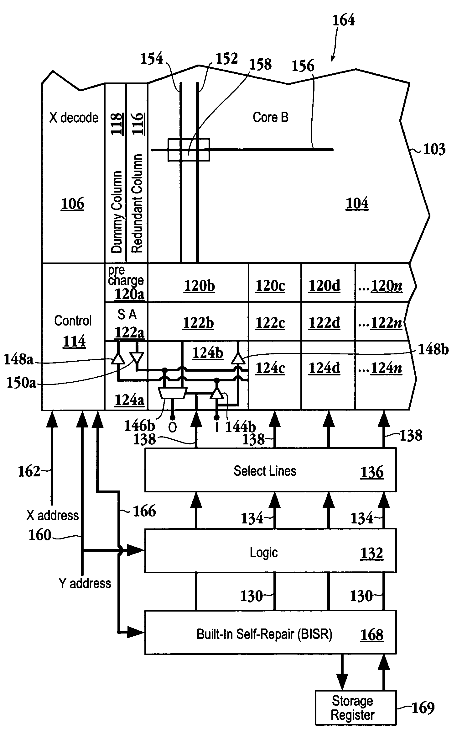
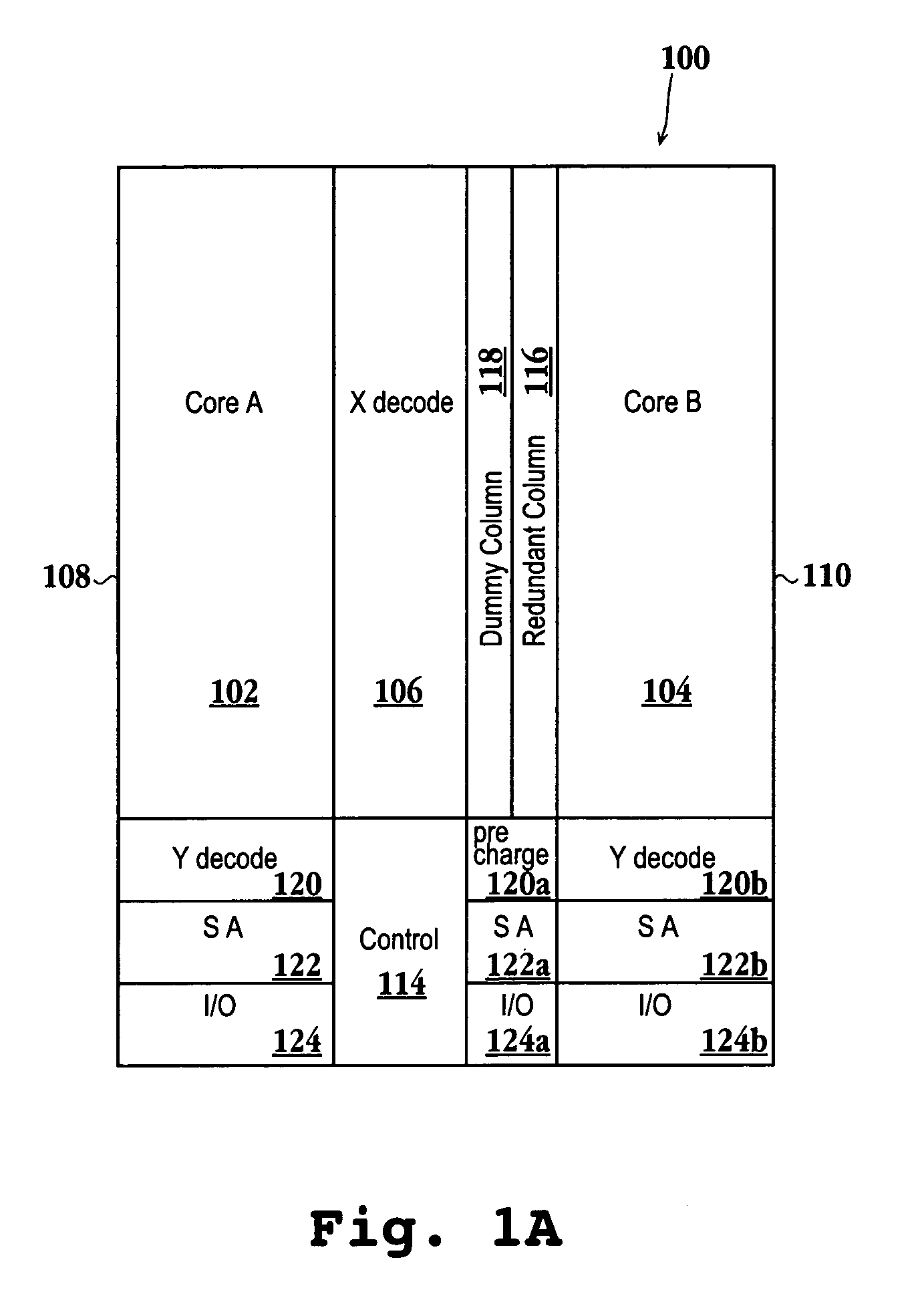
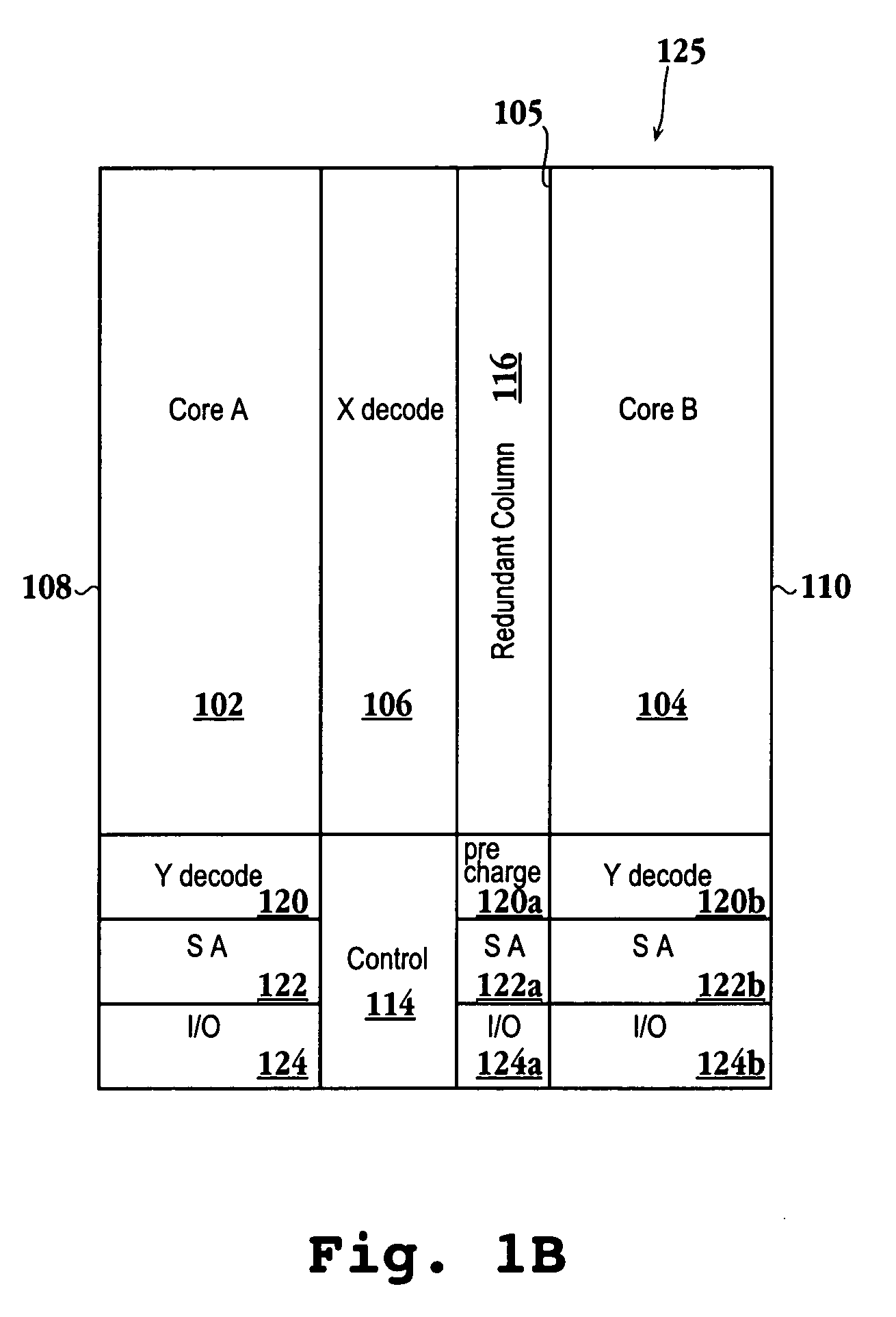
[0031]FIG. 1A illustrates block diagram 100 displaying a split core memory design and associated circuitry in accordance with one embodiment of the invention. Block diagram 100 displays memory Core A 102 and memory Core B 104. It should be appreciated that C...


PUM


Abstract

A column redundancy circuitry and a method for implementing the same are provided. One exemplary method provides routing for an access request addressed to a defective cell. The method includes providing a redundant column within a memory circuit, the redundant column in communication with a sense amplifier. Next, a defective cell of a memory circuit is located and the address is programmed. An access request is then processed, the access request containing the address of the defective cell Finally, the access request is routed to the redundant column through enable circuitry. Some notable advantages include the conservation of surface area of the memory circuit induced by locating the redundant column within the memory circuit. The externalization of the fuse box, Built In Self Repair region and the logic circuitry from the memory core also provide increased flexibility.

Description

CROSS REFERENCE TO RELATED APPLICATIONS[0001]This application claims priority from U.S. Provisional Patent Application No. 60 / 300,497 filed Jun. 22, 2001 and entitled “Memory Column Redundancy Circuitry and Method for Implementing the Same.” This provisional application is herein incorporated by reference.BACKGROUND OF THE INVENTION[0002]1. Field of the Invention[0003]This invention relates generally to integrated circuits and more particularly to circuit structures, methods of use, and apparatus implementing column redundancy in memory architectures.[0004]2. Description of the Related Art[0005]Semiconductor memory cores are typically laid-out in array format. The array structures are typically composed of 2n by 2m individual memory cells which are coupled to wordline (rows) and complementary pair bit lines (columns). A typical memory cell may be composed of transistors coupled together to form a data storage device. An individual memory cell is typically selected when an X-decoder ...

Claims


Application Information

Patent Timeline
IPC IPC(8): G06F11/20G06F12/16G11C29/00G11C29/44
CPCG11C29/44G11C29/4401G11C29/80G11C29/846G11C29/848
Inventor GANDHI, DHRUMIL
Owner ARM INC
Why Eureka
Try Eureka