Investigation device and investigation method

a technology of investigation device and investigation method, which is applied in the direction of image enhancement, semiconductor/solid-state device testing/measurement, instruments, etc., can solve the problem of user difficulty in reviewing itself of a vast amount of inspection image data, and achieve the effect of improving production efficiency and increasing analysis efficiency

Inactive Publication Date: 2005-11-22
HITACHI LTD
View PDF10 Cites 18 Cited by
  • Summary
  • Abstract
  • Description
  • Claims
  • Application Information

AI Technical Summary

Benefits of technology

[0008]An object of the present invention is to provide an inspection device and inspection method which copes with the increase of inspection images and is capable of classification by sub class in addition to the automatic classification by an inspection device in order to meet the user needs.
[0009]The present invention is further capable of reviewing a vast amount of inspection image data and analyzing as much as about 70%, preferably 90% of the images in the classification work in case any defect is found so as to increase the analysis efficiency and improve the production efficiency.

Problems solved by technology

Besides, the review itself of a vast amount of the inspection image data has become tough to the user.

Method used


Image

  • Investigation device and investigation method
  • Investigation device and investigation method
  • Investigation device and investigation method

Examples


Embodiment Construction

[0032]An embodiment according to the present invention is explained hereunder, using the attached figures.

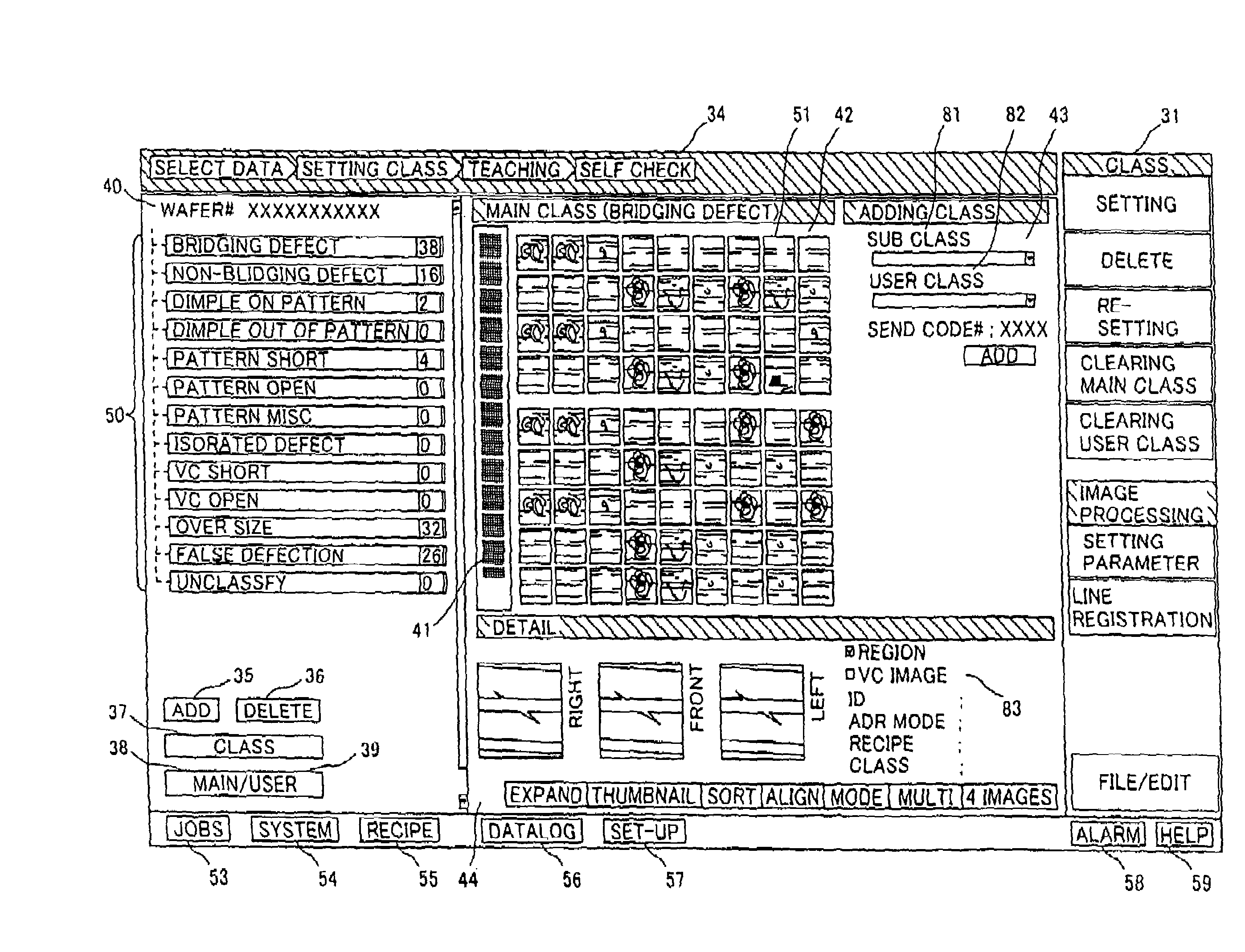
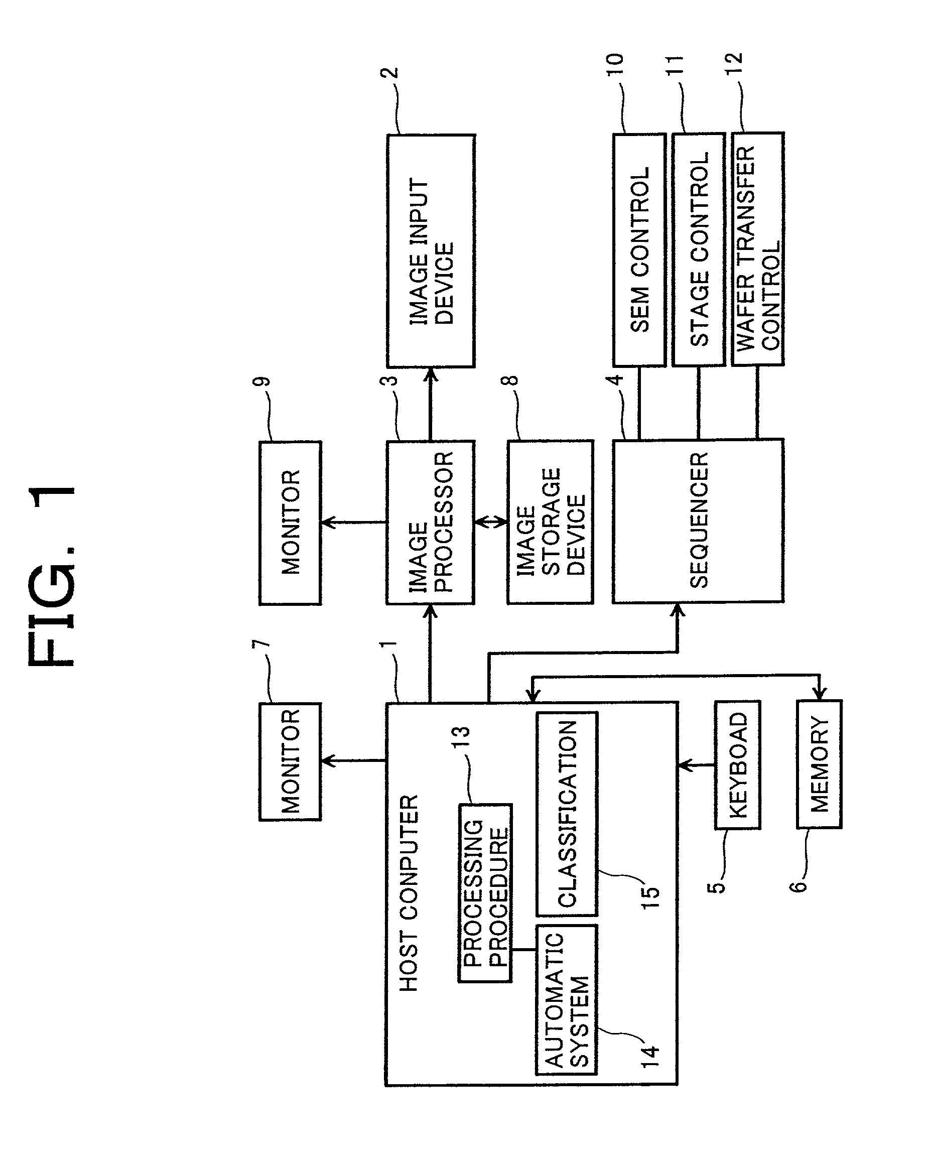
[0033]FIG. 1 is a diagram showing the function blocks of a system which performs the defect inspection of a specimen. This embodiment comprises a host computer 1, image input device 2, image processor 3, sequencer 4, and so on.

[0034]The image input device 2 is equipped with a lighting optical system, comprising an interference optical system, diffraction optical system, slanted lighting optical system, etc., and a photo-taking optical system for forming an inspection image of the specimen on a photo-taking element like CCD. The image of the specimen is taken into the system by the image input device 2.

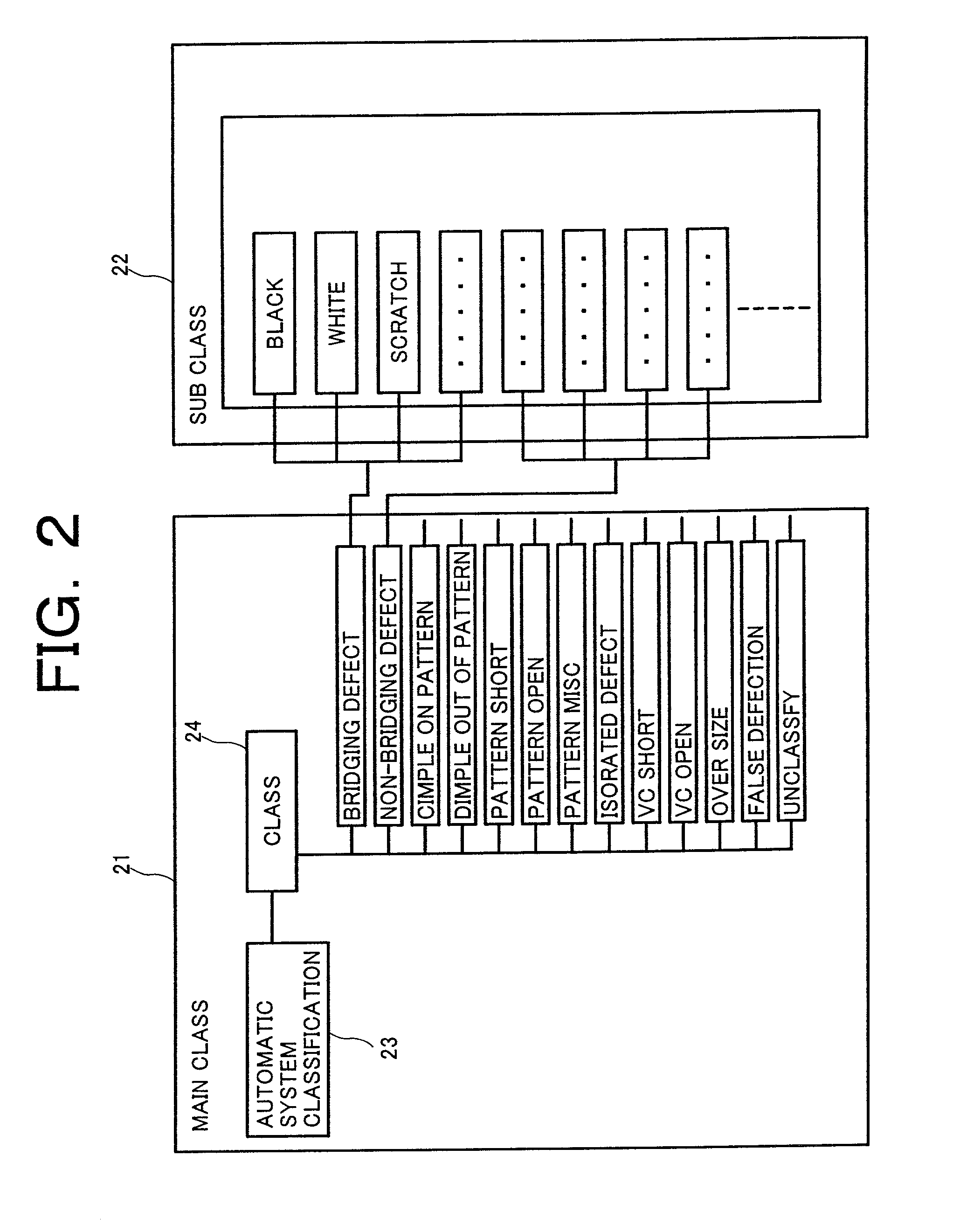
[0035]The image processor 3, connected to the image input device 2, is equipped with an image processing function that extracts defects of the specimen (for example, uneven coating, foreign substance, and dust) from the inputted inspection image and detects the type, quantity, loca...


PUM

PropertyMeasurementUnit
display areaaaaaaaaaaa
areaaaaaaaaaaa
sizeaaaaaaaaaa

Abstract

The present invention relates to an inspection device and inspection method of a specimen, particularly to the inspection device and inspection method of defects of semiconductor wafers, and the object is to cope with the increase of inspection images and provide an inspection device and inspection method which is capable of classification by sub class, meeting the user needs, in addition to the automatic classification by an inspection device.To achieve the afore-mentioned object, the present invention provides an inspection device, comprising a storage means for storing the images obtained and a display means equipped with the first display area for displaying multiple images stored in the storage means and the second display area for displaying the images which are classified according to the characteristics of the displayed images (called the classified images), wherein the display means displays the class of the specimen, displays the sub class which is set manually for each class, and also displays the images selected by the sub class as a mass of the classified images for each sub class.

Description

BACKGROUND OF THE INVENTION[0001]In manufacturing semiconductors, the silicone wafers undergo in-process checks, including foreign substance inspection, visual inspection, and SEM inspection, in each process such as exposure and etching. The inspection images obtained through these inspections are classified and analyzed by size, shape and location of the foreign substance causing a defect and the result is utilized to improve the yield.[0002]A method of classifying these images automatically by characteristics is disclosed in Japanese application patent laid-open publication No. Hei 08-21803. With this method, a classification reference image called “teaching image data” is provided and the images are classified according to this reference image automatically. To be concrete, the Publication covers a defect type judgment device for judging the type of individual defect found through a defect inspection of a specimen; wherein said device is equipped with a neuro-processing unit whic...

Claims


Application Information

Patent Timeline
Patent Type & Authority Patents(United States)
IPC IPC(8): G06T7/00G01N21/956G06T1/00G06T7/60H01L21/66
CPCG06T7/0002G06T7/001G06T7/60G06T2200/24G06T2207/30148
Inventor YOSHIKAWA, AKIRAMACHIDA, KAZUHISAKOMURO, HITOSHIHIRAI, TAKEHIROKITAHASHI, KATSUHIRO
Owner HITACHI LTD
Why Eureka
Try Eureka