Optical interconnection circuit board and manufacturing method thereof

a technology of optical interconnection circuit and manufacturing method, which is applied in the direction of optical elements, semiconductor lasers, instruments, etc., can solve the problems of signal noise and electromagnetic trouble, decrease the operating speed of electronic wiring modules, and loss of transmission wires, so as to reduce manufacturing costs, enhance productivity, and minimize optical coupling loss

Inactive Publication Date: 2005-11-22
KK TOSHIBA
View PDF12 Cites 27 Cited by
  • Summary
  • Abstract
  • Description
  • Claims
  • Application Information

AI Technical Summary

Benefits of technology

[0022]Accordingly, an object of the present invention is to provide an optical connection board and a method of manufacturing the same, each capable of realizing a 90°-optical path transform mechanism that minimizes an optical coupling loss and accomplishes optical termination when the LSIs are mounted on the general-purpose optical connection board, thereby enhance the productivity and reduce the manufacturing cost.

Problems solved by technology

In this regard, it should be noted that the transmission loss in the wires, the signal noise and the electromagnetic trouble increase as the operation clock frequency increases.
Even if the LSIs, which are active devices, can operate high speeds, there is no way but decreasing the operating speed of an electronic wiring module.
Since it takes much time to align the substrates or optical fibers, the productivity of the optical connection module is inevitably lower that that of the electronic wiring module that comprises LSIs.
However, no optical-path angle converters have been realized, which are highly productive and efficient.
With the method of cutting the optical waveguide, however, it is difficult to form an optical input / output portion at any position and in any direction in the substrate.
If many optical input / output portions are provided, the productivity will decrease.
In the method of mounting external mirrors, not only the substrate becomes complicated, but also mounting failure or pollution is likely to occur because these mirrors are mechanically mounted.
The problems described above hamper an increase in the productivity of the optical connection modules, rendering it difficult to manufacture highly general-purpose optical connection modules at low cost.
However, the active devices are buried in the mounting substrate, the structure can hardly enlarged to tens of centimeters due to thermal distortion, and wiring for the mounting is not suitable for general purpose.
This conventional structure is disadvantageous in that the energy loss in the guided light wave is too large.
Generally, converging light beam results in an increase in the divergent angle of the beam.
Here arises the problem that optical coupling efficiency of the optical transmission portion may fall in some cases.
This problem cannot help but be accepted as necessity.
Nonetheless, it leads to an energy loss in the optical transmission of a one-way distribution of signal.
This generates a delay noise signal.
Consequently, the process of controlling the unevenness and the depth therefore is complicated, and the manufacturing method is difficult to control.
However, it requires a large initial investment for the mold, and the wiring pattern cannot be altered easily.
As described above, in the optical connection board for optically connecting LSIs, a highly practical 90°-optical path transform mechanism has not been yet realized.
The productivity cannot be raised, and the manufacturing cost cannot be lowered.

Method used


Image

  • Optical interconnection circuit board and manufacturing method thereof
  • Optical interconnection circuit board and manufacturing method thereof
  • Optical interconnection circuit board and manufacturing method thereof

Examples


first embodiment

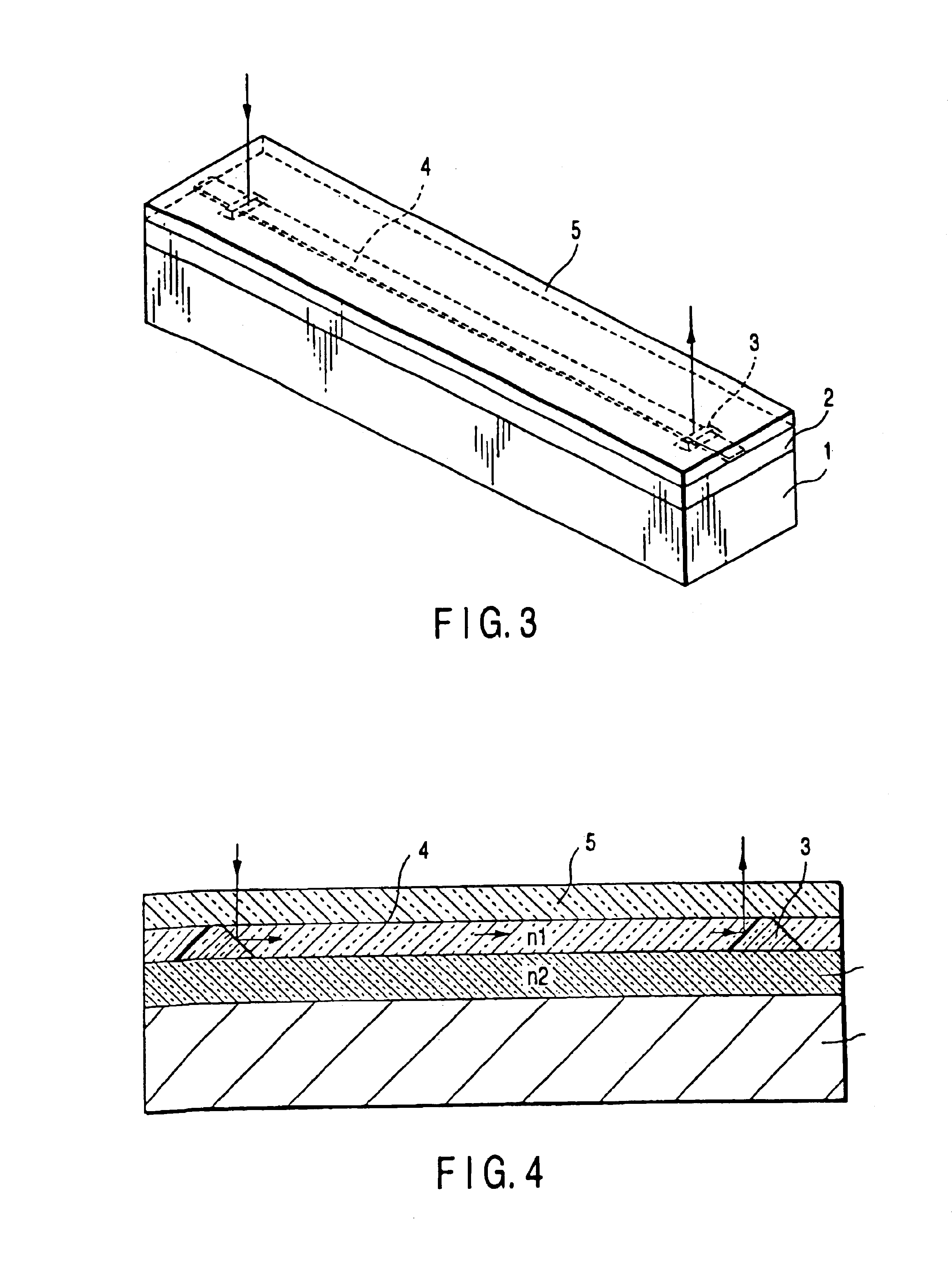
[0087]First, an optical connection board according to the invention will be described with reference to FIGS. 3 and 4.

[0088]As FIG. 3 shows, the optical connection board comprises a substrate 1 having a flat surface, a lower clad layer 2 having a refractive index n2 and formed on the flat surface of the substrate 1, a termination mirror 3 formed on a flat surface of the lower clad layer 2, an optical waveguide core 4 having a refractive index n1 and formed on the flat surface of the lower clad layer 2, and an upper clad layer 5 having the refractive index n2 and formed on the flat surfaces of the optical waveguide core 4 and the termination mirror 3. The lower clad layer 2, or the first clad layer, is provided on the substrate 1, for confining a light wave or optical signal in the core 4. The termination mirror 3 is a hollow member having a reflection face. The mirror 3 may be filled with a refractive member or metal to form a reflector having a reflection face. The optical waveguid...

second embodiment

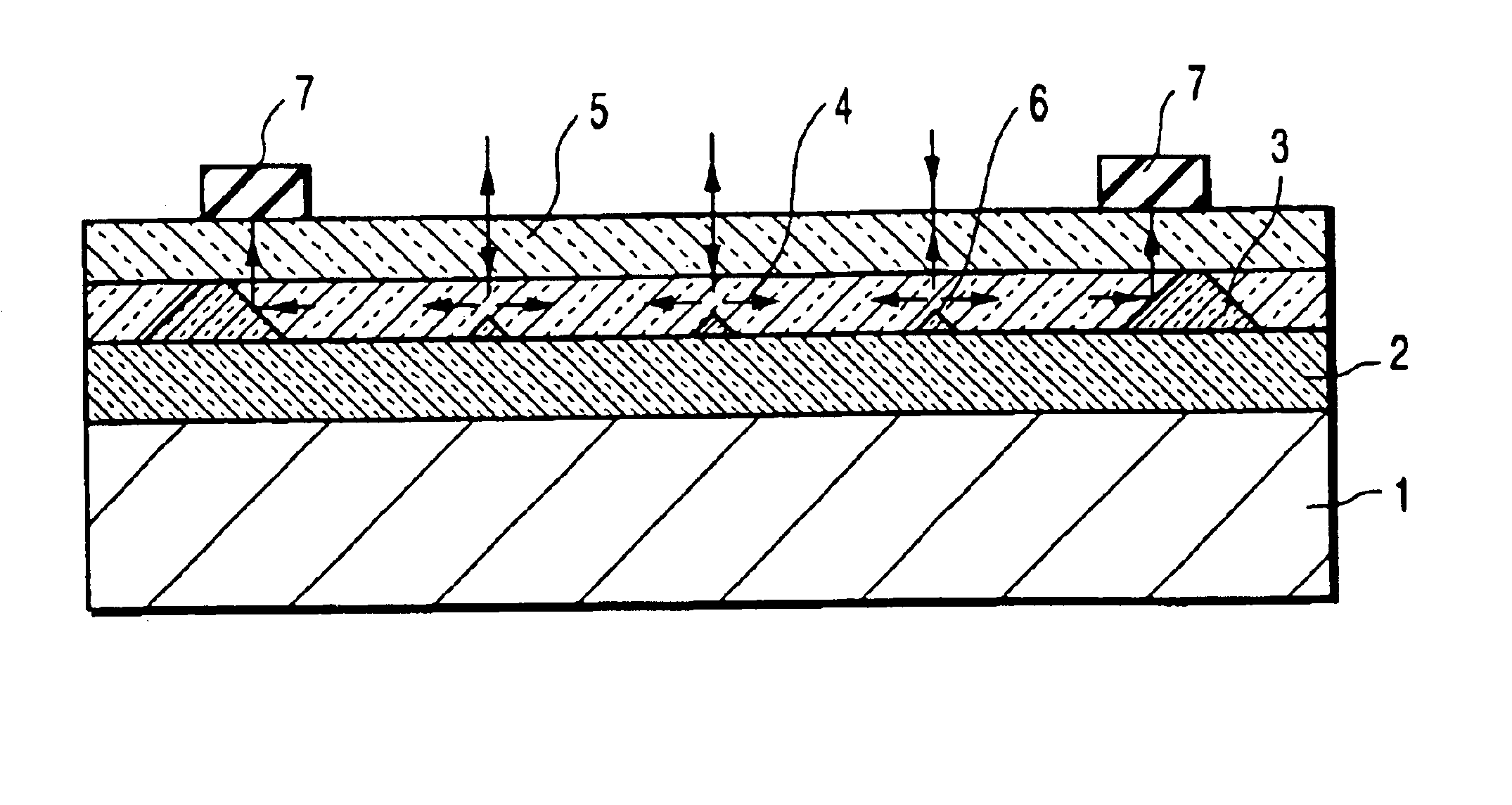
[0094]The optical connection board will be described with reference to FIGS. 5 and 6. FIG. 5 shows part of the optical interconnection circuit board. FIG. 6 is a sectional view, taken along the axis of the optical waveguide core 4. The component similar to those shown in FIGS. 3 and 4 are designated at the same reference numerals, and will not described in detail.

[0095]In the optical connection board of FIGS. 5 and 6, three mirrors 6 are provided between two termination mirrors 3, for splitting an input optical signal. Each split mirror 6 has a face inclined at about 45° to the signal-guiding direction of the optical waveguide, like the termination mirror 3. The mirrors 6 extend across the optical waveguide core 5. The mirrors 6 have a small height than the optical waveguide core 5, unlike the termination mirror 3. In other words, their height is smaller than the thickness of the core 5. Thus, a core region for guiding the optical signal is provided over the mirrors 6. As a result,...

third embodiment

[0099]An optical connection board according to the invention will be described with reference to FIG. 7.

[0100]FIG. 7 is a sectional view showing part of the third embodiment of the present invention. The components identical to those shown in FIG. 6 are denoted at the same reference numerals will not be described in detail.

[0101]As shown in FIG. 7, the optical connection board comprises a light-absorbing segment 7 for absorbing unnecessary optical signal. The light-absorbing segment 7 is provided on the upper clad layer 5, to absorb optical signal reflected from the termination mirror 3. The other components are of the same structure as those of the first and second embodiments. The light-absorbing segment 7 may be formed by an appropriate material selected in accordance with the wavelength of the optical wave that may be applied to it. If the light applied to it has wavelength of 0.85 μm, the segment 7 may be made of semiconductors such as Si or Ge, or polymer containing carbon or ...


PUM


Abstract

In an optical connection board, a first clad layer is formed on a flat surface of a substrate and a core layer is formed on the first clad layer and is extended in a propagation direction of an optical signal. The core layer is covered with a second clad layer. A termination mirror having a reflection face is so buried in the clad layer as to reflect the optical signal guided in the core layer, to the outside of the optical connection board.

Description

CROSS-REFERENCE TO RELATED APPLICATIONS[0001]This Application is a Divisional Application of Ser. No. 09 / 961,372 filed on Sep. 25, 2001 now U.S. Pat. No. 6,741,781.[0002]This application is based upon and claims the benefit of priority from the prior Japanese Patent Application No. 2000-301062, filed Sep. 29, 2000, the entire contents of which are incorporated herein by reference.BACKGROUND OF THE INVENTION[0003]1. Field of the Invention[0004]The present invention relates to an optical interconnection circuit board and a method of manufacturing the circuit board. More particularly, the invention relates to an optical interconnection circuit board having an optical waveguide for optically connecting different LSIs at high speeds and to a method of manufacturing the circuit board.[0005]2. Description of the Related Art[0006]Recently, electronic devices as bipolar transistors and field-effect transistors have been improved in terms of their performance. The clock frequency of the LSI h...

Claims


Application Information

Patent Timeline
Patent Type & Authority Patents(United States)
IPC IPC(8): G02B6/43G02B6/125G02B6/12G02B6/42G02B6/122G02B6/13H01S5/00H01S5/20
CPCG02B6/125G02B6/43G02B6/42G02B6/4214G02B2006/12069G02B2006/12104G02B2006/12176H01S5/20
Inventor FURUYAMA, HIDETO
Owner KK TOSHIBA
Why Eureka
Try Eureka