
Method of forming photodiode with self-aligned implants for high quantum efficiency

a self-aligned, photodiode technology, applied in the direction of semiconductor devices, radio frequency controlled devices, electrical apparatus, etc., can solve the problems of poor signal to noise ratio of cmos imagers, affecting the physical and electrical properties of pinned layers, and affecting the magnitude of dark current generated

Active Publication Date: 2005-11-29
APTINA IMAGING CORP
View PDF1 Cites 24 Cited by
  • Summary
  • Abstract
  • Description
  • Claims
  • Application Information

AI Technical Summary

Benefits of technology

[0019]These and other features and advantages of the invention will be more apparent from the following detailed descript

Problems solved by technology

In addition, defects and trap sites inside or near the photodiode depletion region strongly influence the magnitude of dark current generated.
Mask misalignment may occur as a result of using several masks and this, in turn, affects the physical and electrical properties of the pinned layer.
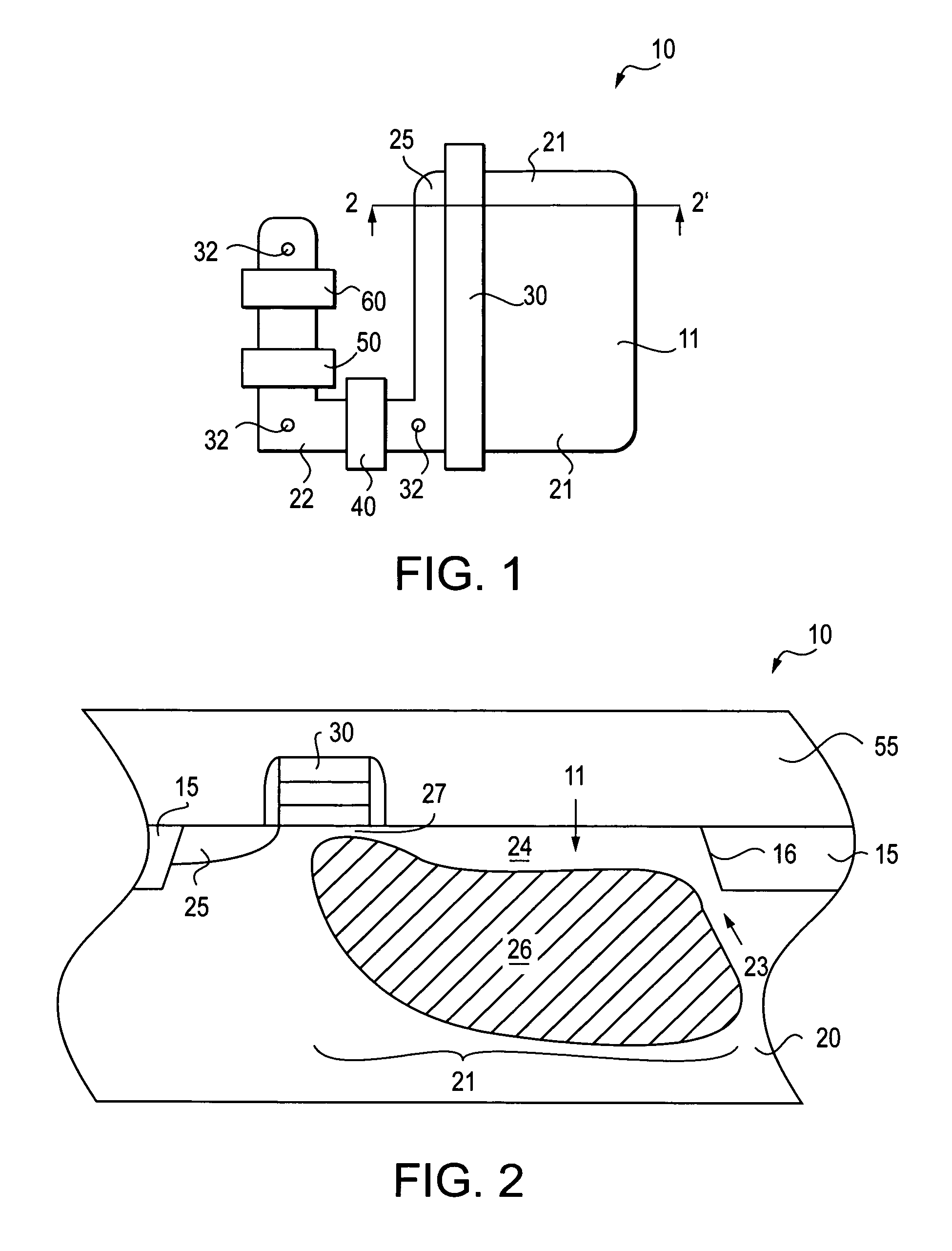
CMOS imagers also typically suffer from poor signal to noise ratios and poor dynamic range as a result of the inability to fully collect and store the electric charge collected in the region 26.

Method used


Image

  • Method of forming photodiode with self-aligned implants for high quantum efficiency
  • Method of forming photodiode with self-aligned implants for high quantum efficiency
  • Method of forming photodiode with self-aligned implants for high quantum efficiency

Examples


Embodiment Construction

[0034]In the following detailed description, reference is made to the accompanying drawings which form a part hereof, and in which is shown by way of illustration specific embodiments in which the invention may be practiced. These embodiments are described in sufficient detail to enable those skilled in the art to practice the invention, and it is to be understood that other embodiments may be utilized, and that structural, logical and electrical changes may be made without departing from the spirit and scope of the present invention.

[0035]The terms “wafer” and “substrate” are to be understood as a semiconductor-based material including silicon-on-insulator (SOI) or silicon-on-sapphire (SOS) technology, doped and undoped semiconductors, epitaxial layers of silicon supported by a base semiconductor foundation, and other semiconductor structures. Furthermore, when reference is made to a “wafer” or “substrate” in the following description, previous process steps may have been utilized ...


PUM


Abstract

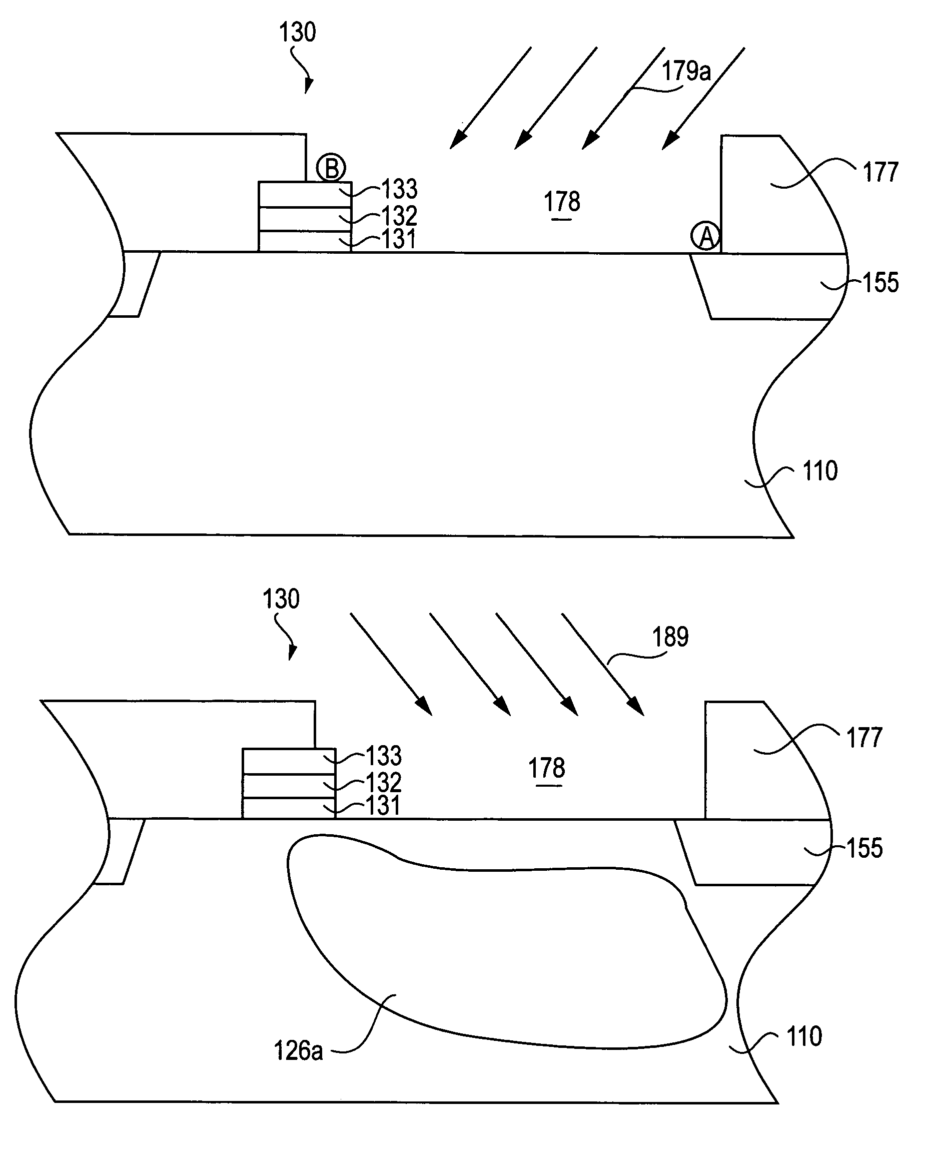
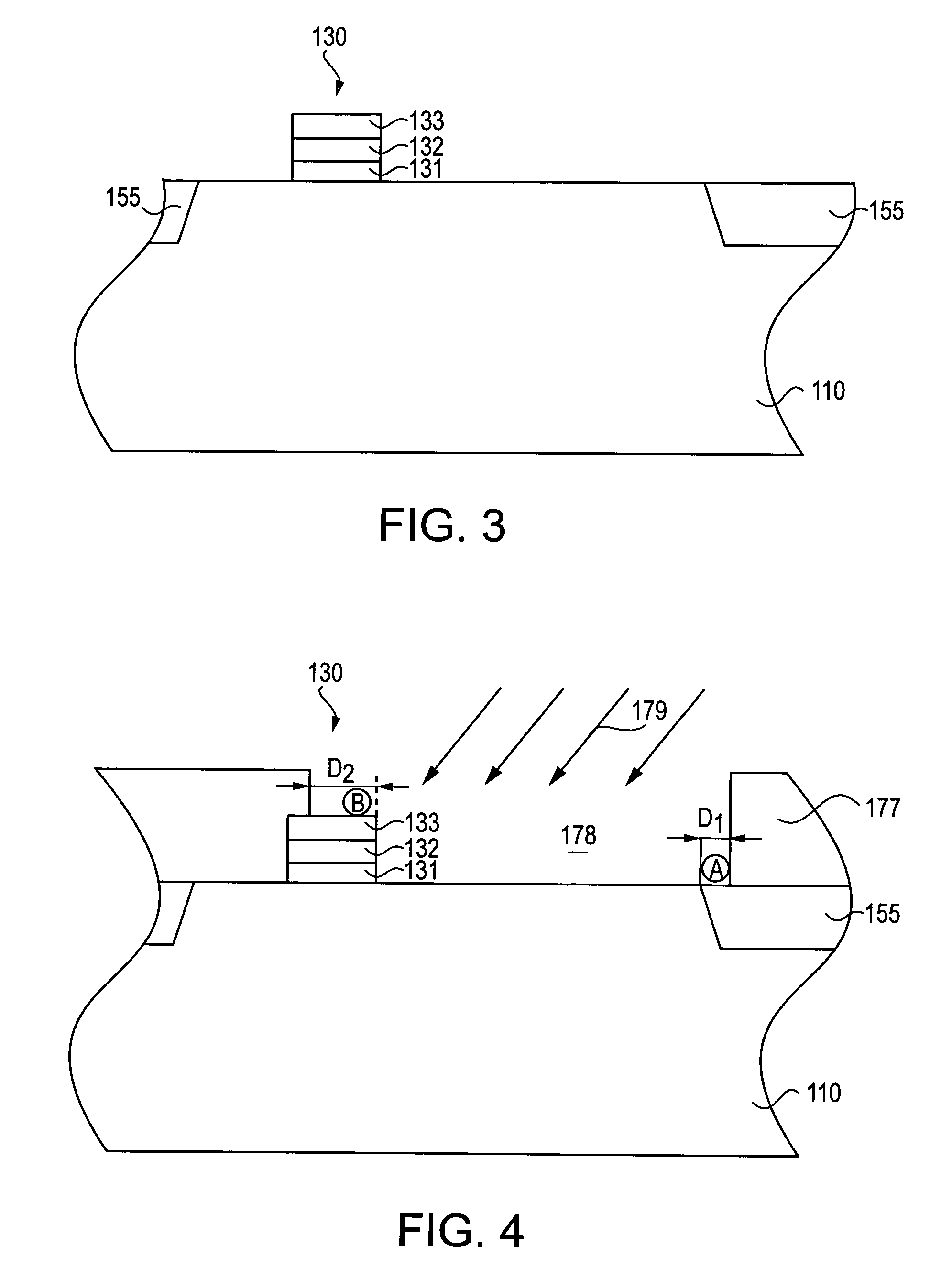
A pinned photodiode with a pinned surface layer formed by a self-aligned angled implant is disclosed. The angle of the implant may be tailored to provide an adequate offset between the pinned surface layer and an electrically active area of a transfer gate of the pixel sensor cell. The pinned surface layer is formed by employing the same mask level as the one employed for the formation of the photodiode region, and then implanting dopants at angles other than zero degrees.

Description

CROSS-REFERENCE TO RELATED APPLICATION[0001]This application claims priority of provisional application Ser. No. 60 / 478,348 filed Jun. 16, 2003, the entire disclosure of which is incorporated herein by reference.FIELD OF THE INVENTION[0002]The present invention relates to the field of semiconductor devices and, in particular, to improved photodiodes for high quantum efficiency.BACKGROUND OF THE INTENTION[0003]The semiconductor industry currently uses different types of semiconductor-based imagers, such as charge coupled devices (CCDs), photodiode arrays, charge injection devices and hybrid focal plane arrays, among others.[0004]Because of the inherent limitations and expense of CCD technology, CMOS imagers have been increasingly used as low cost imaging devices. A CMOS imager circuit includes a focal plane array of pixel cells, each one of the cells including either a photodiode, a photogate or a photoconductor overlying a doped region of a substrate for accumulating photo-generated...

Claims


Application Information

Patent Timeline
IPC IPC(8): H01L21/00H01L27/146H01L27/15H01L31/062
CPCH01L27/14601H01L27/14603H01L27/14609H01L27/14689
Inventor MOULI, CHANDRARHODES, HOWARD
Owner APTINA IMAGING CORP
Learn More