Method of fabricating strained Si SOI wafers

a technology of strained silicon and substrate, which is applied in the manufacturing of semiconductor/solid-state devices, basic electric elements, electric devices, etc., can solve the problems of affecting the production efficiency of ssoi, and having an intrinsic complication

Inactive Publication Date: 2005-12-06
IBM CORP
View PDF2 Cites 17 Cited by
  • Summary
  • Abstract
  • Description
  • Claims
  • Application Information

AI Technical Summary

Problems solved by technology

In addition, the intervening SiGe layer causes additional complication in processes such as, for example, enhanced N-type dopant diffusion, Si / SiGe intermixing, shallow trench isolation (STI) process complications, and possible negative effects on silicide formation.
This prior method has an intrinsic complication because wafer bonding requires very smooth surfaces, and graded SiGe films have a very rough surface which makes SiGe films not suitable for use in most wafer bonding processes.
CMP is used in the prior art method to make the surfaces smoother, but CMP reduces the substrate manufacturability, especially for 300 mm wafers.
The main drawbacks to the abovementioned concept are 1) the questionable ability to grow high-quality thick relaxed SiGe alloy layers with low-enough defect density, 2) the questionable ability to recrystallize through a very thick random alloy without generating new defects, 3) the practical challenge of amorphizing such a large buried region with a conventional implant procedure and 4) minimizing the interdiffusion of Ge into the lower Si layer during all these processing steps.

Method used


Image

  • Method of fabricating strained Si SOI wafers
  • Method of fabricating strained Si SOI wafers
  • Method of fabricating strained Si SOI wafers

Examples


Embodiment Construction

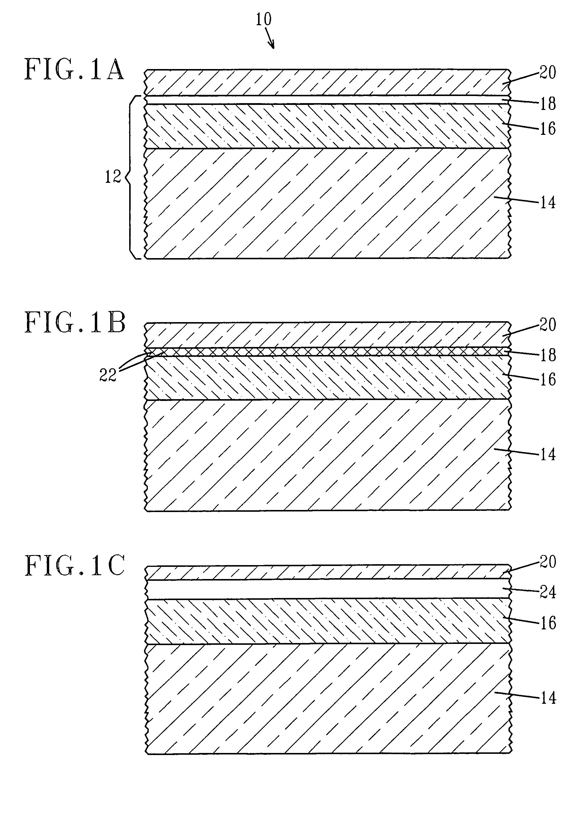
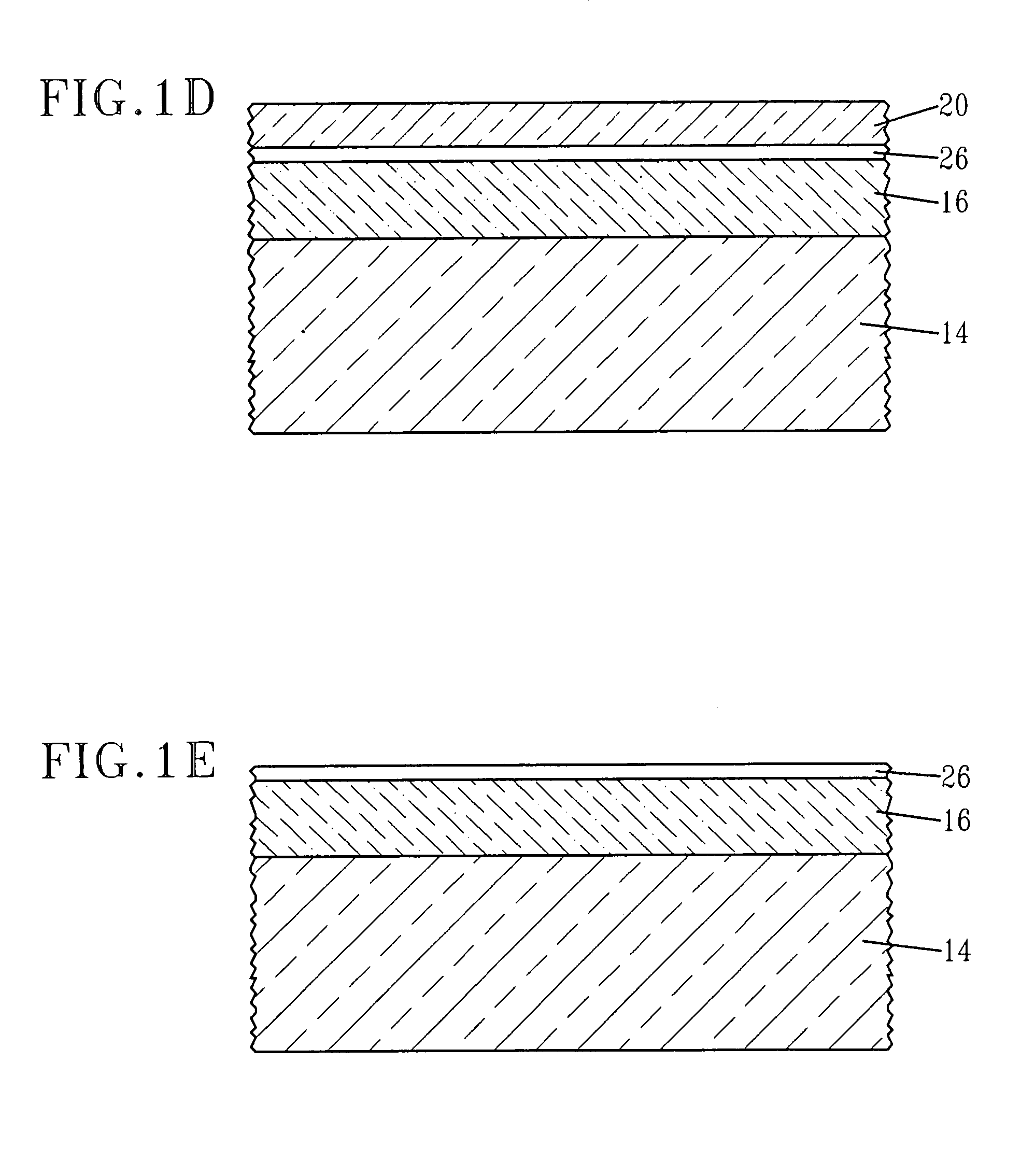
[0019]The present invention, which provides a method for forming a strained semiconductor-on-insulator substrate, will now be described in greater detail by referring to the drawings that accompany the present application. It is noted that the drawings of the present invention are not drawn to scale therefore the present application is not limited to any dimensions that may be ascertained from the drawings. Moreover, in the accompanying drawings, like reference numerals are employed for describing like and / or corresponding elements.

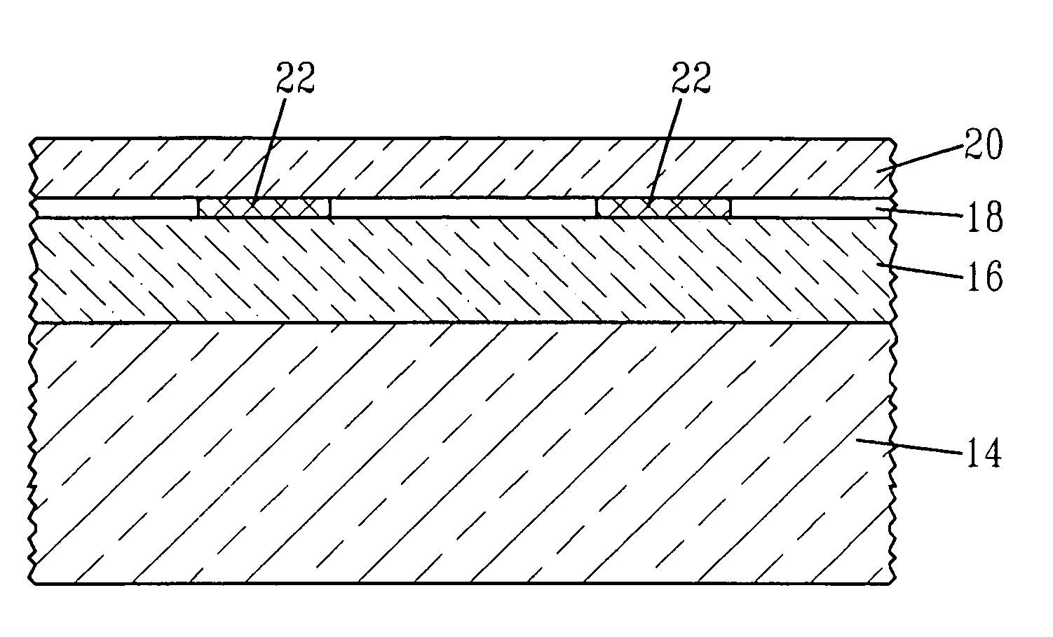
[0020]Reference is first made to FIG. 1A which illustrates a structure 10 that is provided after forming a second crystalline semiconductor layer 20 on a surface of a first crystalline semiconductor layer 18. The first crystalline semiconductor layer 18 represents the topmost layer of a preformed SOI substrate 12. The first semiconductor layer 18 is oftentimes referred to in the art as an SOI layer wherein electrical devices such as, for example, transist...


PUM

PropertyMeasurementUnit
thicknessaaaaaaaaaa
thicknessaaaaaaaaaa
temperatureaaaaaaaaaa

Abstract

A method of fabricating a strained semiconductor-on-insulator (SSOI) substrate in which the strained semiconductor is a thin semiconductor layer having a thickness of less than 50 nm that is located directly atop an insulator layer of a preformed silicon-on-insulator substrate is provided. Wafer bonding is not employed in forming the SSOI substrate of the present invention.

Description

FIELD OF THE INVENTION[0001]The present invention relates to a method of fabricating a semiconductor substrate, and more particularly to a method of fabricating a strained semiconductor-on-insulator (SSOI) substrate.BACKGROUND OF THE INVENTION[0002]Strained Si has been adopted as a promising option to improve complementary metal oxide semiconductor (CMOS)-based transistor device performance. Typically, Si is deposited on a layer of relaxed SiGe to produce a Si layer that is under tensile strain. Strained Si on SiGe has also been used in conjunction with silicon-on-insulator (SOI) to combine the benefits of both technologies. In some applications, it would be ideal to have a strained Si layer directly over an insulating layer without an intervening SiGe layer; this will allow an ultra thin SOI layer which is consistent with the current trend of SOI technology development. In addition, the intervening SiGe layer causes additional complication in processes such as, for example, enhance...

Claims


Application Information

Patent Timeline
Patent Type & Authority Patents(United States)
IPC IPC(8): H01L21/20H01L21/324H01L21/762
CPCH01L21/324H01L21/20
Inventor BEDELL, STEPHEN W.COHEN, GUY M.CHEN, HUAJIE
Owner IBM CORP
Why Eureka
Try Eureka