Light emitting diode with porous SiC substrate and method for fabricating

a technology of light-emitting diodes and sic substrates, which is applied in the direction of basic electric elements, semiconductor devices, electrical equipment, etc., can solve the problems of limited external quantum efficiency, difficult to create a useful roughened surface, and the emission region formed of a sic substrate cannot include useful roughened surfaces on the sic substrate to enhance light extraction, etc., to achieve the effect of improving the extraction of led ligh

Inactive Publication Date: 2005-12-06
CREELED INC
View PDF9 Cites 70 Cited by
  • Summary
  • Abstract
  • Description
  • Claims
  • Application Information

AI Technical Summary

Benefits of technology

[0011]The present invention seeks to provide a method and apparatus for forming a porous layer on the surface of a semiconductor material, with the semiconductor material then being used as a substrate for an LED. The porous layer is arranged to improve extraction of the LED light that passes through the substrate.
[0015]A light emitting diode (LED) package according to the present invention comprises an LED having a substrate with a porous layer on one or more surfaces and an emission region formed on a surface of the substrate not having a porous layer. The package further comprises a metal layer with the LED flip-chip mounted to the metal layer such that the substrate becomes the primary emission surface of said LED. At least two contacts are included for applying a bias across the emission region, causing the emission region to emit light omnidirectionally. The porous layer enhances light extraction of emission region light passing through the substrate.

Problems solved by technology

For conventional LEDs with a single out-coupling surface, the external quantum efficiency is limited by total internal reflection (TIR) of light from the LED's emission region that passes through the substrate.
It has proven difficult to create a useful roughened surface on SiC and it is believed that these difficulties are caused by the chemically inert nature of SiC.
Accordingly, a LED formed of an emission region on a SiC substrate can not include useful roughened surfaces on the SiC substrate to enhance light extraction.
The backside surfaces of SiC substrates have been lapped to in an attempt to provide a useful level of roughness, but these attempts have met with limited success and did not result in a LED with significantly enhanced light extraction.

Method used


Image

  • Light emitting diode with porous SiC substrate and method for fabricating
  • Light emitting diode with porous SiC substrate and method for fabricating
  • Light emitting diode with porous SiC substrate and method for fabricating

Examples


Embodiment Construction

Aparatus and Method for Forming Porous Layer

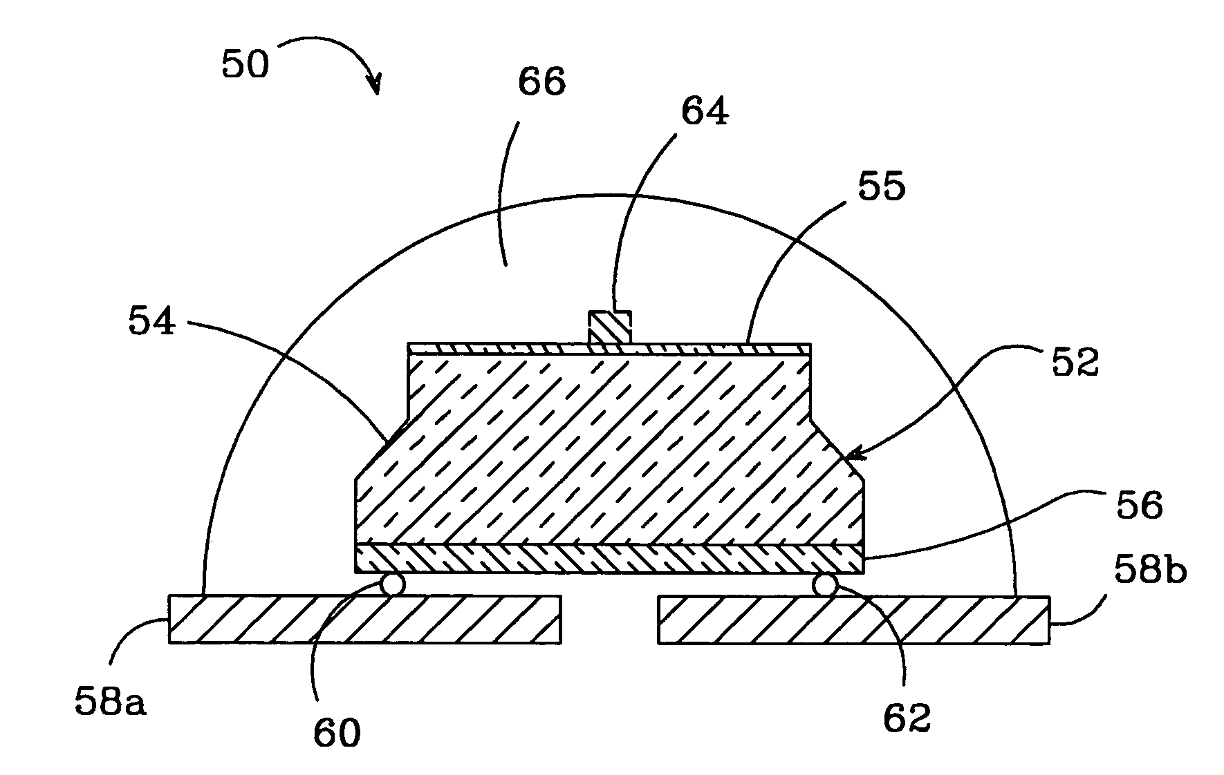
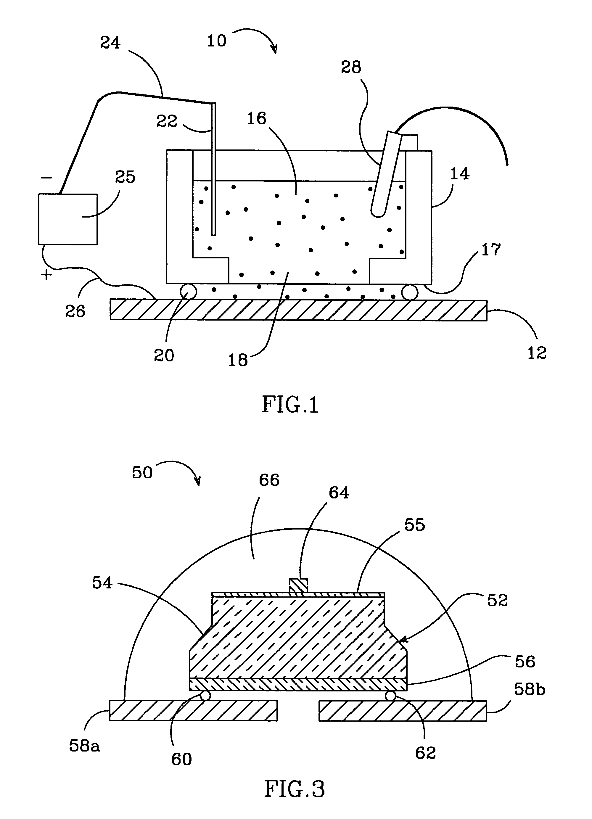
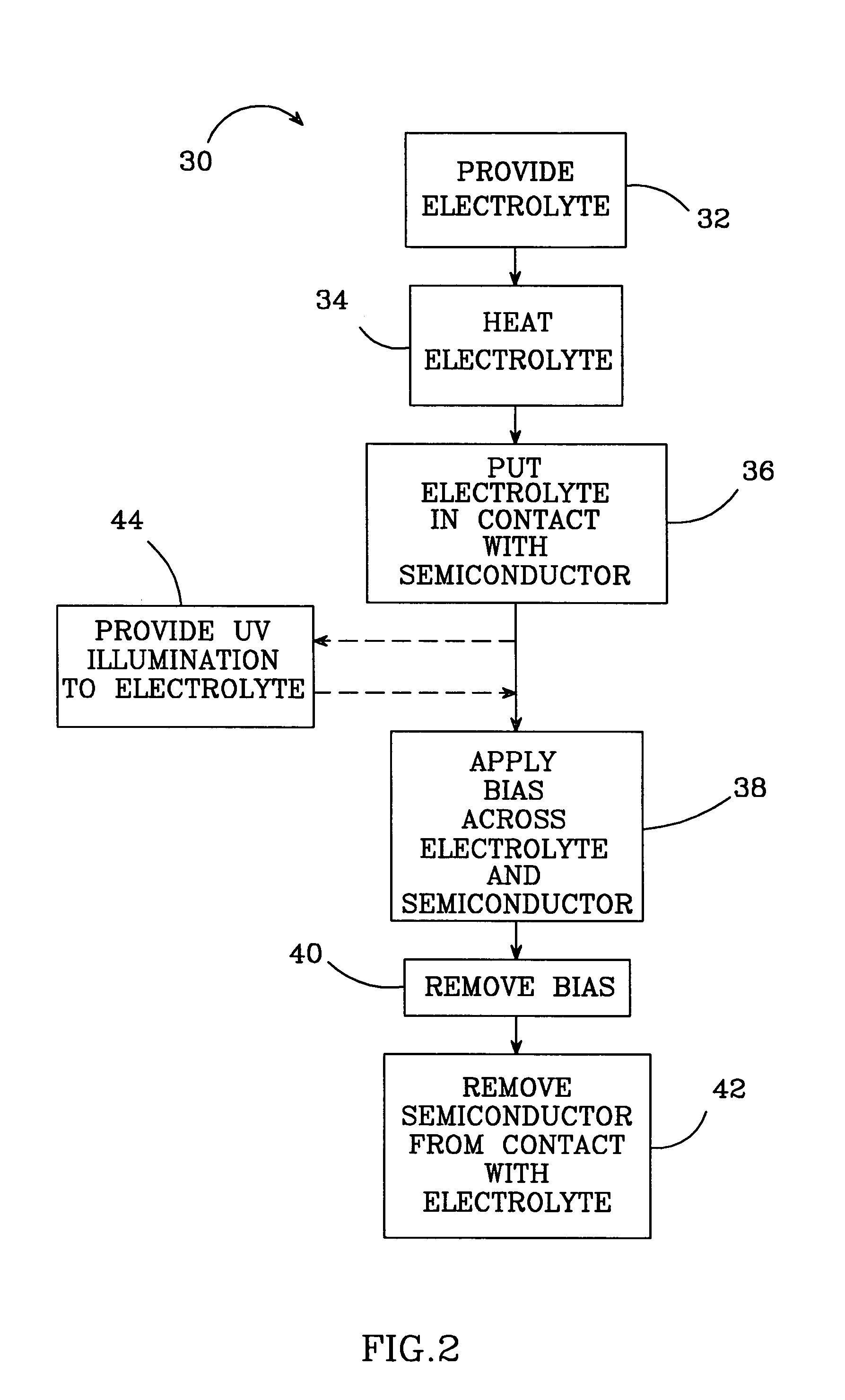
[0024]FIG. 1 shows one embodiment on an apparatus 10 according to the present invention for forming a porous layer on the surface of a semiconductor material 12, with the apparatus 10 preferably used to form a porous layer on the surface of silicon carbide (SiC). The apparatus 10 includes a cup shaped reservoir / housing 14 holding a liquid HF-based electrolyte 16 that can comprise different solutions in different concentrations. A suitable solution for the electrolyte 16 comprises ethanol (C2H5OH) and water, with ethanol in a concentration range of a 10 to 50%. Another suitable solution comprises a buffered HF-based electrolyte that provides for a more constant Ph value over time and provides for a solution that is less volatile and less dangerous to work with. A preferred buffered HF-based electrolyte comprises ammonium fluoride (NH4F) and water, with the NH4F having different concentrations such as 20% per volume.

[0025]The semiconductor 1...


PUM

PropertyMeasurementUnit
External Quantum Efficiencyaaaaaaaaaa
voltageaaaaaaaaaa
voltageaaaaaaaaaa

Abstract

A method and apparatus for forming a porous layer on the surface of a semiconductor material wherein an electrolyte is provided and is placed in contact with one or more surfaces of a layer of semiconductor material. The electrolyte is heated and a bias is introduced across said electrolyte and the semiconductor material causing a current to flow between the electrolyte and the semiconductor material. The current forms a porous layer on the one or more surfaces of the semiconductor material in contact with the electrolyte. The semiconductor material with its porous layer can serve as a substrate for a light emitter. A semiconductor emission region can be formed on the substrate. The emission region is capable of emitting light omnidirectionally in response to a bias, with the porous layer enhancing extraction of the emitting region light passing through the substrate.

Description

[0001]This invention was made with Government support under the Department of Energy (NETL) Contract No. DE-FC26-00NT40985. The Government has certain rights in this inventionBACKGROUND OF THE INVENTION[0002]1. Field of the Invention[0003]This invention relates to semiconductor based light emitters, and more particularly to light emitting diodes comprising an emission region formed on a substrate.[0004]2. Description of the Related Art[0005]Light emitting diodes (LEDs) are an important class of solid state devices that convert electric energy to light and generally comprise an active layer of semiconductor material sandwiched between two oppositely doped layers. When a bias is applied across the doped layers, holes and electrons are injected into the active layer where they recombine to generate light. Light is emitted omnidirectionally from the active layer and from all surfaces of the LED.[0006]There has been a great deal of recent interest in LEDs formed of Group-III nitride base...

Claims


Application Information

Patent Timeline
Patent Type & Authority Patents(United States)
IPC IPC(8): H01L21/3063H01L31/0236H01L33/16H01L33/20
CPCH01L21/3063H01L33/20H01L33/16H01L31/0236H01L2924/10158H01L2224/16245
Inventor LI, TINGIBBETSON, JAMESKELLER, BERND
Owner CREELED INC
Why Eureka
Try Eureka