EMC/ESD mitigation module

Active Publication Date: 2005-12-06
AVAYA INC
View PDF6 Cites 25 Cited by
  • Summary
  • Abstract
  • Description
  • Claims
  • Application Information

AI Technical Summary

Benefits of technology

[0007]These and other needs are addressed by the various embodiments and configurations of the present invention. The present invention provides a mitigation module that provides

Problems solved by technology

Although this approach reduces certain types of electric-field radiation, it compromises compliance with certain ESD/EMC requirements.
The PCB's robustness against ESD discharges is compromised because the metal standoffs provide a low-impedance path.
This coupling allows ESD currents to flow from the

Method used


Image

  • EMC/ESD mitigation module
  • EMC/ESD mitigation module
  • EMC/ESD mitigation module

Examples


first embodiment

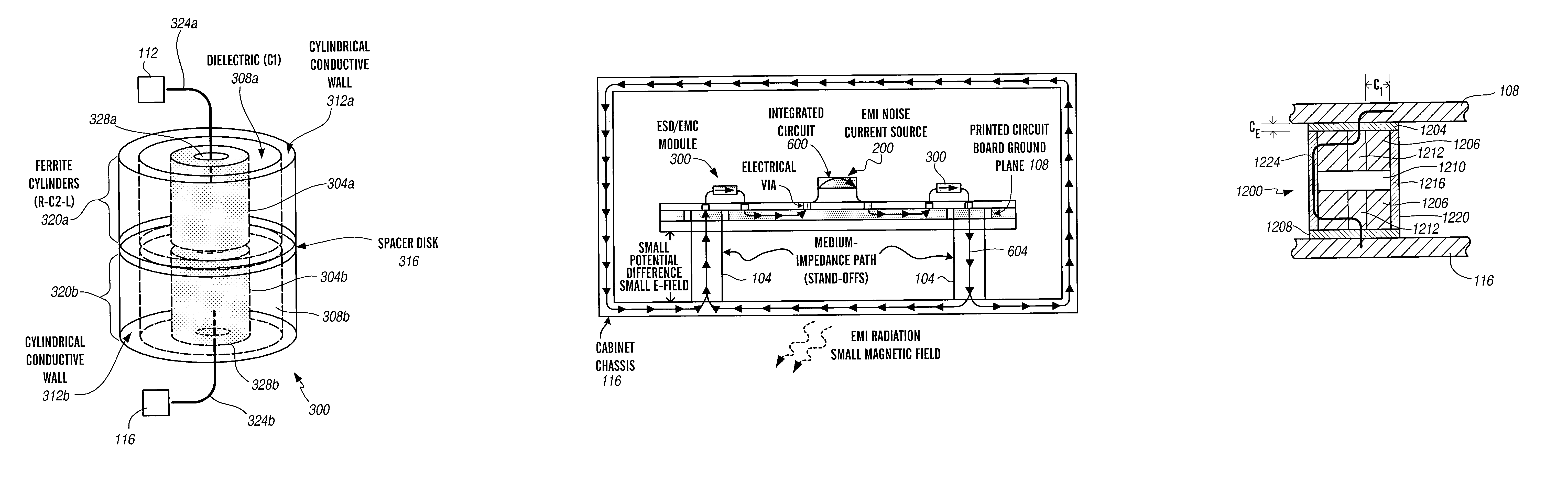
[0029]FIGS. 3 and 4 depict a cylindrical through-hole mitigation module according to the present invention. The mitigation module 300 comprises first and second (co-axially aligned) ferrite cores 304a and b, first and second (co-axially aligned) dielectric materials 308a and b surrounding the peripheries of the first and second ferrite cores 304a and b, respectively, first and second (co-axially aligned) outer conductive (e.g., metal) shells 312a and b surrounding the peripheries of the first and second dielectric materials 308a and b, respectively, and a conductive (e.g., metal) annular spacer disk 316 positioned between the first and second sections 320a and b of the module. The first and second ferrite cores 304a and b, first and second dielectric materials 308a and b, first and second outer conductive shells 312a and b, and conductive spacer disk 316 are, in one configuration, co-axially aligned along line 324.

[0030]The electrical behavior of the module 300 is depicted in FIG. 5...

second embodiment

[0040]FIG. 10 shows a module according to the present invention that is particularly useful as a surface mountable module design that can be used in a tape-and-reel installation technique. The module 1000 comprises co-axially aligned (continuous) ferrite core 1004, dielectric material 1008, first and second outer conductive shells 1012a and b, and insulative (annular) spacer ring 1016. A washer-shaped air gap 1010 (or insulative material) exists that is coplanar with the insulative annular ring. This air gap physically separates the two dielectric materials of the two capacitors and provides a much smaller capacitance than that capacitance provided by the conductive shell-dielectric-ferrite structure. As will be appreciated, the air gap 1010 and ring 1016 can be placed by a washer-shaped insulative annular ring extending from the outer surface of the shells 1012a and b to the outer surface of the core 1004. This design can be more manufacturable than an air gap and provide a high de...

third embodiment

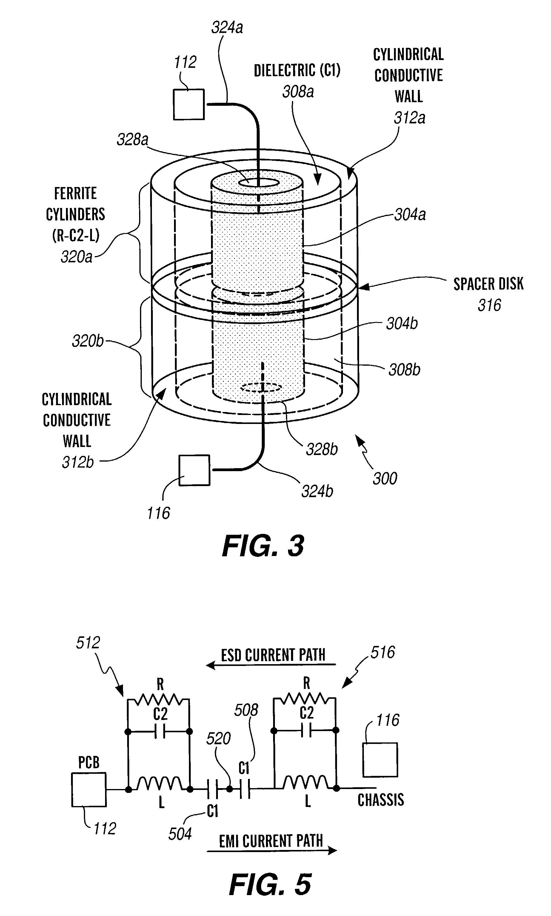
[0044]FIG. 11 depicts a PCB mounting design according to the present invention. In the design, the PCB ground plane 108 is in contact with standoff 1100, which in turn is in contact with the chassis 116. The first and second sections 1104a and 1104b of the standoff are electrically conductive while the central section 1110 of the standoff is electrically insulating. The mitigation module 300 or 1100 is positioned adjacent to the central section 1108 and is in electrical contact with the first and second sections 1104a and 1104b. This configuration of components produces the electromagnetic current path 1108 shown.


PUM


Abstract

An assembly for mitigating at least one of an electrostatic discharge and electromagnetic interference is provided. The assembly includes (a) first and second spaced apart electrical conductors 108 and 116 and (b) a mitigation module 300 electrically coupled to the first and second spaced apart electrical conductors to control a magnitude of an electrostatic discharge and/or electromagnetic interference in the first and second electrical conductors 108 and 116. One or more of the following statements is true: (i) the mitigation module 300 comprises a ferrite material 304; (ii) the mitigation module 300 comprises a lossy dielectric material 308; and (iii) an equivalent electrical circuit for at least part of the mitigation module 300 comprises at least a first circuit segment 512 comprising a first inductor and a first capacitor electrically connected in parallel and a second capacitor 504 electrically connected in series with the first circuit segment 512. The first and second electrical conductors can be, for example, a ground plane of a printed circuit board 108 and a wall of the enclosure or chassis 116.

Description

FIELD OF THE INVENTION[0001]The present invention relates generally to modules for protecting electronic devices from electromagnetic energy and specifically to a module for protecting printed circuit boards (PCBs) from electrostatic discharge (ESD) and electromagnetic incompatibility.BACKGROUND OF THE INVENTION[0002]Printed circuit boards (PCBs) housed within metal enclosures must comply with electrostatic discharge (ESD) and electromagnetic compatibility (EMC) requirements. To comply with these requirements, the PCBs must not malfunction in the presence of electrical discharges that are coupled onto the metal enclosures, and the PCBs must not emit excessive radiation outside of the metal enclosures.[0003]In an EMC compliance approach, the PCBs ground plane(s) are electrically connected to the enclosure's chassis, thereby reducing electric-field radiation. The interconnection of the ground plane with the chassis equalizes potential differences that may exist between the PCB and the...

Claims


Application Information

Patent Timeline
IPC IPC(8): H05K1/02H05K9/00
CPCH05K9/0067H05K1/0233
Inventor NORTE, DAVID A.YOON, WOONG K.TRAN, THU-DUYEN NGOC
Owner AVAYA INC
Why Eureka
Try Eureka