Eureka AIR delivers breakthrough ideas for toughest innovation challenges, trusted by R&D personnel around the world.

Method for fabricating copper interconnects

a technology of copper interconnects and manufacturing methods, applied in semiconductor/solid-state device manufacturing, basic electric elements, electric apparatus, etc., can solve the problems of poor adhesion of copper, short circuit, silicon nitride,

Inactive Publication Date: 2005-12-20
TAIWAN SEMICON MFG CO LTD
View PDF14 Cites 28 Cited by
  • Summary
  • Abstract
  • Description
  • Claims
  • Application Information

AI Technical Summary

Benefits of technology

[0013]The present invention provides methods to form copper silicide as a capping layer of copper interconnects.

Problems solved by technology

Although Cu or Cu alloy interconnects have superior properties for applications, there are drawbacks in Cu implementation.
For example, Cu readily diffuses into dielectric layers, particularly silicon dioxide, which results in electrical shorts.
The drawback of silicon nitride is poor adhesion to copper.
The subsequent process usually causes silicon nitride to peel away from the copper plugs.
The peeled silicon nitride creates a path for copper to diffuse outward and for moisture or contaminates to diffuse inward and thus degrade reliability of the interconnects.

Method used


Image

  • Method for fabricating copper interconnects
  • Method for fabricating copper interconnects
  • Method for fabricating copper interconnects

Examples


Embodiment Construction

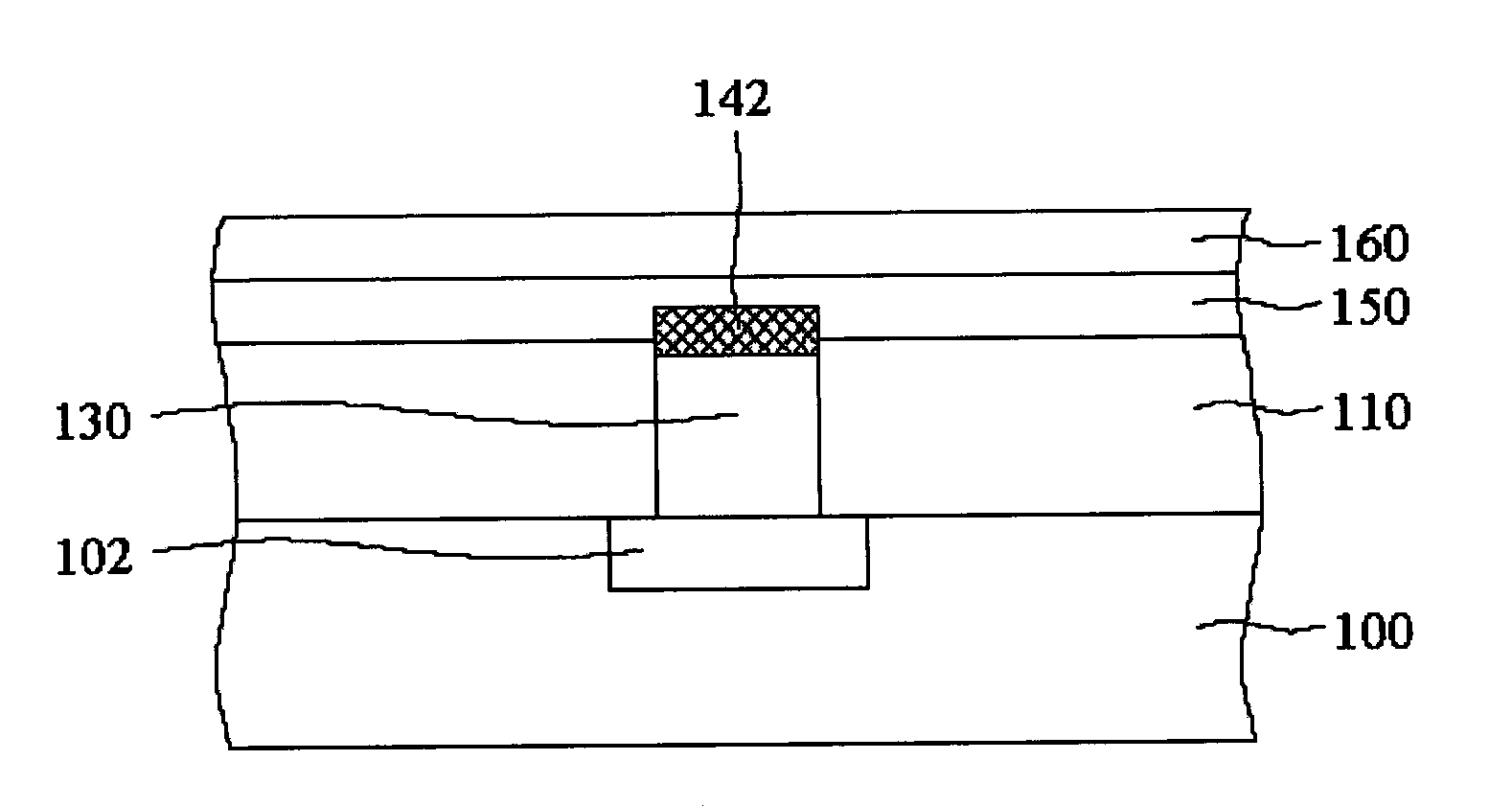
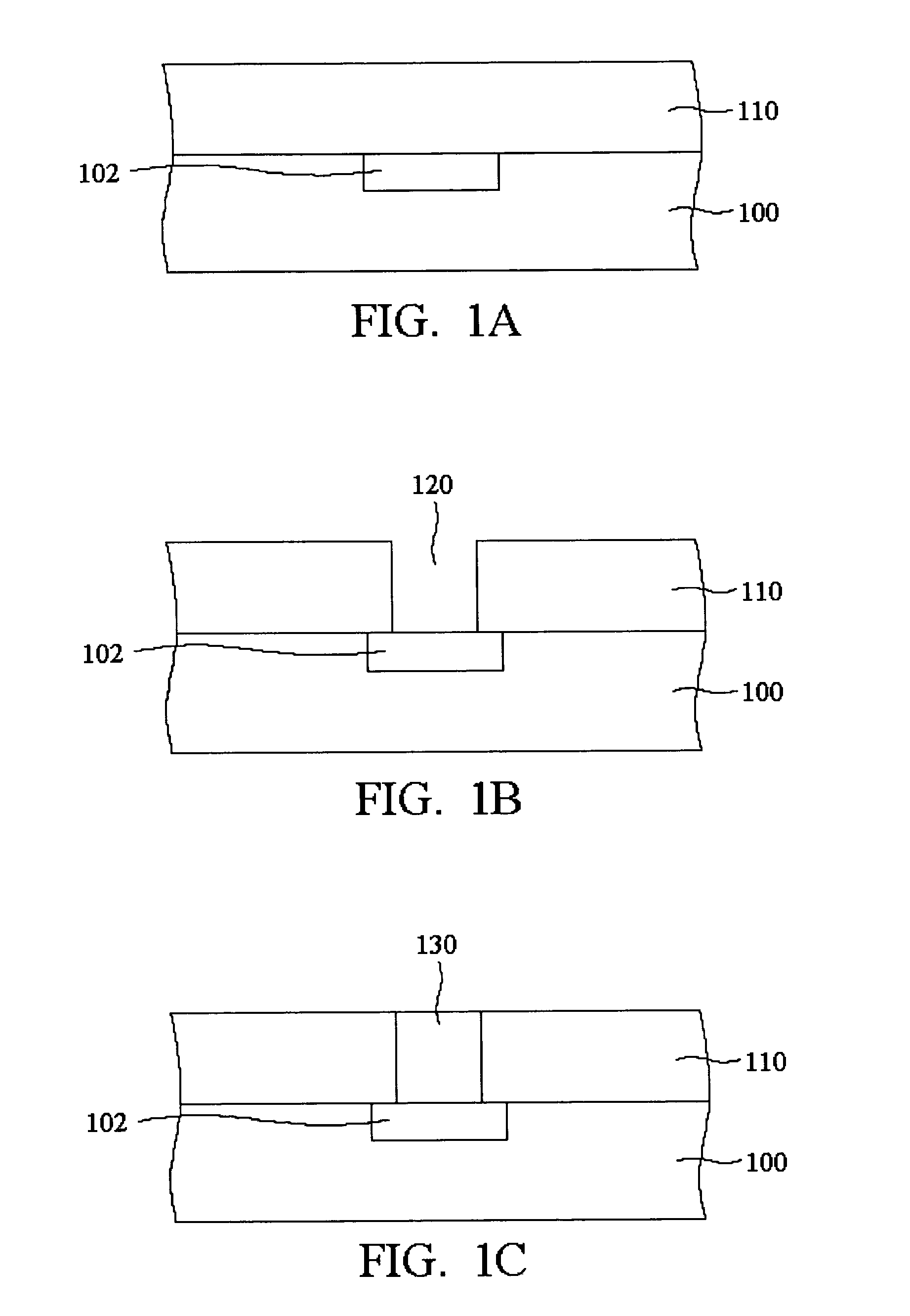
[0018]In FIG. 1A, a semiconductor substrate 100 is provided with a conductive structure 102 thereon, such as a gate electrode or a metal line. A dielectric layer 110 is deposited overlying the semiconductor substrate 100. The preferred dielectric layer 110 is low-k material (k≦3.2), such as organic low-k material, CVD low-k material, or a combination thereof The dielectric layer can also be fluorinated silica glass (FSG), SiC, SiOC, SiOCN, carbon-containing silicon oxide or nitrogen-containing silicon oxide.

[0019]A damascene opening 120 is subsequently formed within the dielectric layer 110 to expose the underlying conductive structure 102 as shown in FIG. 1B. The preferred width of the opening 120 is less than 900 Å. Preferably, the opening 120 is defined by a conventional dual damascene process to form a trench and a via opening.

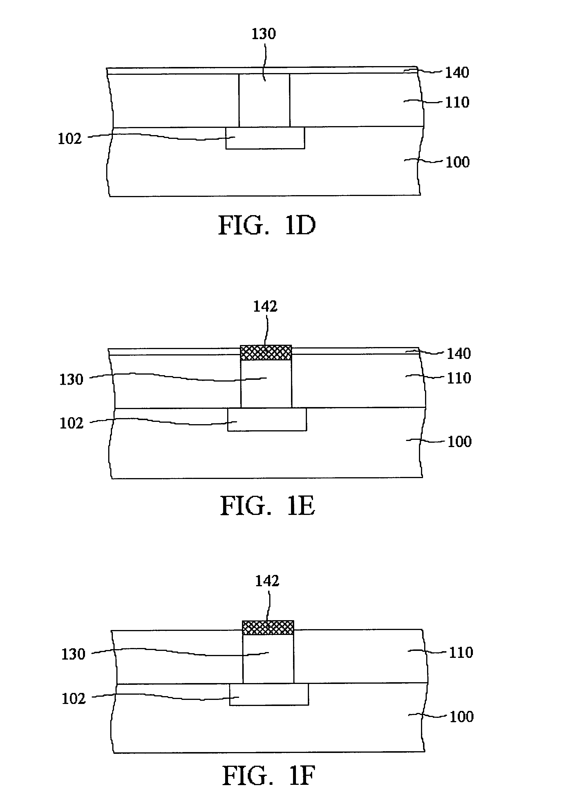
[0020]The opening 120 is filled with copper or copper alloy to form a copper plug 130, as FIG. 1C shows. In one embodiment, a diffusion barrier layer (not...


PUM

PropertyMeasurementUnit
widthaaaaaaaaaa
thicknessaaaaaaaaaa
temperatureaaaaaaaaaa

Abstract

A method for capping copper or copper alloy interconnects. A dielectric layer is formed overlaying a semiconductor substrate. An opening is formed in the dielectric layer and subsequently embedded copper or copper alloy form an interconnect structure. A silicon layer is formed on the copper or copper alloy by sputtering or chemical vapor deposition. A copper silicide layer is formed by reacting the silicon layer with the underlying copper or copper alloy as a capping layer.

Description

BACKGROUND OF THE INVENTION[0001]1. Field of the Invention[0002]The present invention relates to semiconductor fabrication, and in particular to methods for capping copper interconnects in semiconductor devices.[0003]2. Description of the Related Art[0004]Conventional semiconductor devices comprise conductive interconnects to establish electric contact with conductive structures inside semiconductor substrates. Interconnects comprise metal lines and metal plugs formed in dielectric layers for horizontal and vertical connections.[0005]High performance semiconductor applications require rapid speed in semiconductor circuitry. The speed of semiconductor circuitry varies inversely with the resistance and capacitance of the interconnection pattern. As integrated circuits become more complex and feature size and space become smaller, the integrated circuit speed becomes more dependent upon the interconnect pattern, and thus, materials utilized in interconnect structures have become a majo...

Claims


Application Information

Patent Timeline
Patent Type & Authority Patents(United States)
IPC IPC(8): H01L21/768
CPCH01L21/76849H01L21/76867
Inventor YU, CHEN-HUATSENG, HORNG-HUEI
Owner TAIWAN SEMICON MFG CO LTD
Why Eureka
Eureka Blog
Learn More