Fiber incorporating quantum dots as programmable dopants

a fiber and quantum dots technology, applied in the field of fiber incorporating quantum dots as programmable dopants, can solve the problems of no means or pathways by which these quantum dots particles can be stimulated electrically, the quantum dots have no doping characteristics, and the film is extremely fragil

Inactive Publication Date: 2005-12-20
RAVENBRICK
View PDF15 Cites 69 Cited by
  • Summary
  • Abstract
  • Description
  • Claims
  • Application Information

AI Technical Summary

Benefits of technology

[0023]In some embodiments of the present invention, the excitation level of the artificial atom is also controlled, either through additional electrical voltages or through optical or electromagnetic stimulation. Additionally, in some embodiments of the invention the energy in the control paths creates electric fields which affect the quantum confinement characteristics of the quantum dots, producing controlled and repeatable distortions in the size and shape of the artificial atoms, further altering their doping characteristics, with a corresponding effect on the surrounding materials. Since the electrical, optical, thermal, magnetic, mechanical, and chemical properties of a material depend on its electronic structure, and since the embedding of dopants can affect this structure, the programmable dopant fiber offers a means of controlling the interior properties of bulk materials in real time.
[0027]According to the present invention, the programmable dopant fiber can be used outside of bulk materials, in applications where quantum dots, quantum wires, and nanoparticle films are presently used. For example, the programmable dopant fiber can serve as a microscopic light source or laser light source that is both long and flexible. Further, multiple programmable dopant fibers can be arranged on a surface to produce two-dimensional materials analogous to nanoparticle films, but much stronger.

Problems solved by technology

However, these films are extremely fragile, and are “three dimensional” only in the sense that they have been made up to several microns thick.
However, there is no means or pathway by which these quantum dot particles can be stimulated electrically.
Thus, the doping characteristics of the quantum dots are fixed at the time of manufacture and cannot be adjusted thereafter.
However, there is virtually no prior art discussing the use, placement, or control of programmable quantum dots in the interior of bulk materials.
Similarly, there is no prior art discussing the placement of quantum dots on the surface of an electrically or optically conductive fiber.
In addition, no means is described for exciting the quantum dots electrically.
Unfortunately, the two-dimensional nature of the electrodes means that the artificial atom can exist only at or near the surface of the wafer, and cannot serve as a dopant to affect the wafer's interior properties.
Such a chip also suffers from the limitation cited in the previous paragraph: its two-dimensional structure prevents its being used as a dopant except near the surface of a material or material layer.

Method used


Image

  • Fiber incorporating quantum dots as programmable dopants
  • Fiber incorporating quantum dots as programmable dopants
  • Fiber incorporating quantum dots as programmable dopants

Examples


Embodiment Construction

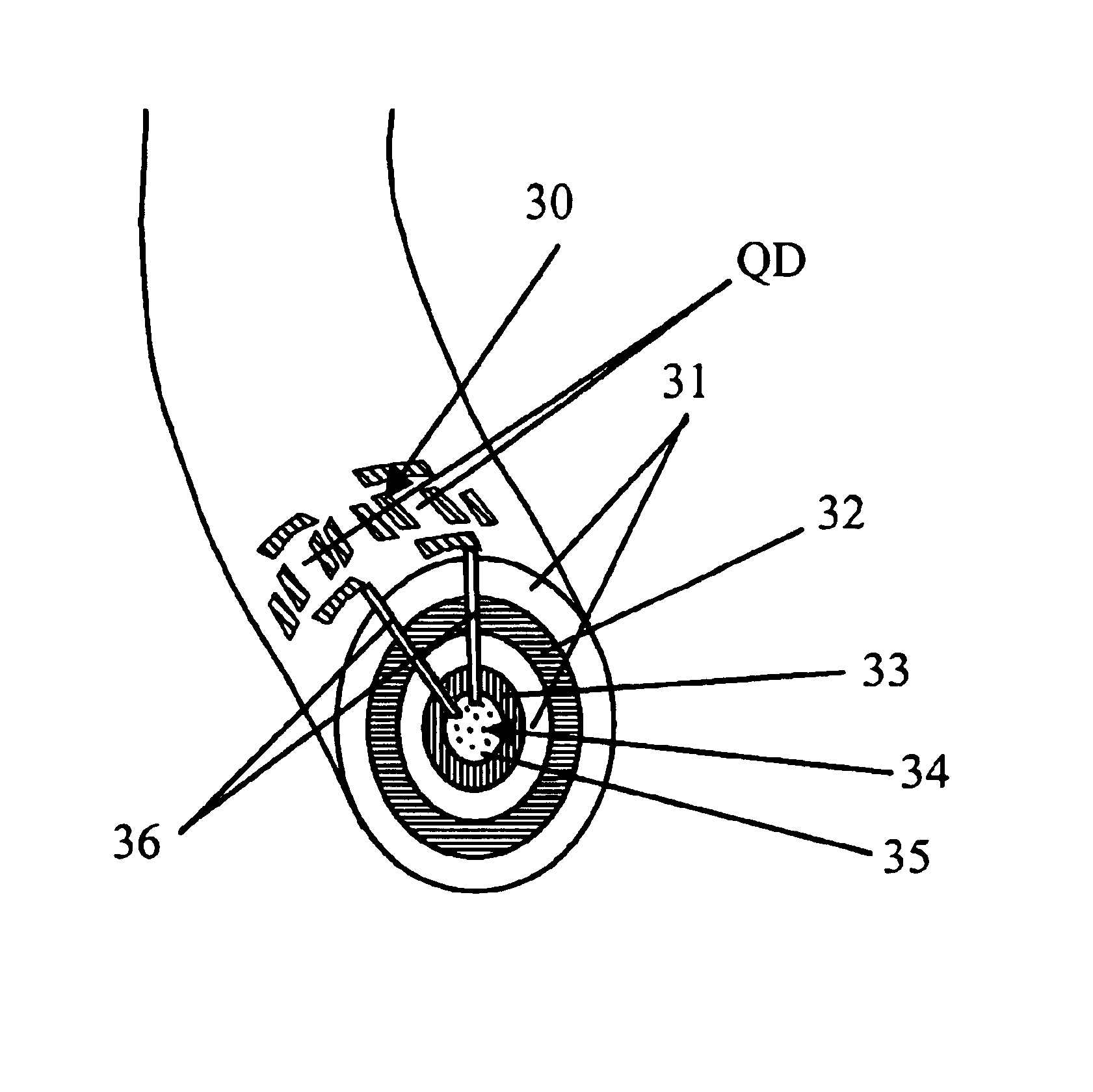
[0037]FIGS. 4a (isometric view) and 4b (end view) show a preferred embodiment of the invention, which is a fiber containing control wires (34) in an insulating medium (35), surrounded by a quantum well, plus an optional memory layer (33). The preferred composition of the insulator (35) is a semiconductor oxide, although a variety of other materials could be used. The preferred composition of the quantum well is a central or transport layer (32) of a semiconductor (similar to the negative layer of a P-N-P junction), for example, GaAs, surrounded by barrier or supply layers (31) of a semiconductor with higher conduction energy (similar to the positive layers of a P-N-P junction). Because of the difference in conduction energies, electrons “fall” preferentially into the lower energy of the transport layer (32), where they are free to travel horizontally (that is, within the layer) but are confined vertically (perpendicular to the layer) by the higher conduction energy of the barrier la...


PUM

PropertyMeasurementUnit
carry energyaaaaaaaaaa
sizeaaaaaaaaaa
shapeaaaaaaaaaa

Abstract

A programmable dopant fiber includes a plurality of quantum structures formed on a fiber-shaped substrate, wherein the substrate includes one or more energy-carrying control paths (34), possibly surrounded by an insulator (35), which pass energy to quantum structures. Quantum structures may include quantum dot particles (37) on the surface of the fiber or electrodes (30) on top of barrier layers (31) and transport layer (32) which form quantum dot devices (QD). The energy passing through the control paths (34) drives charge carriers into the quantum dots (QD), leading to the formation of “artificial atoms” with real-time tunable properties. These artificial atoms then serve as programmable dopants, which alter the behavior of surrounding materials. The fiber can be used as a programmable dopant inside bulk materials, as a building block for new materials with unique properties, or as a substitute for quantum dots or quantum wires in certain applications.

Description

CROSS-REFERENCE TO RELATED APPLICATIONS[0001]This application is entitled to the benefit of Provisional Patent Application No. 60 / 312,264, filed Aug. 14, 2001.BACKGROUND OF THE INVENTION[0002]1. Field of the Invention[0003]This invention relates to a device for producing quantum effects, namely a fiber that is capable of carrying energy with an exterior surface populated by quantum dot structures that are controlled by changes in the energy carried by the fiber. The invention has particular, but not exclusive, application in materials science as a programmable dopant that can be placed inside bulk materials and controlled by external signals.[0004]2. Description of the Related Art[0005]The fabrication of very small structures to exploit the quantum mechanical behavior of charge carriers (e.g., electrons or electron “holes”) is well established. Quantum confinement of a carrier can be accomplished by a structure whose linear dimension is less than the quantum mechanical wavelength of...

Claims


Application Information

Patent Timeline
Patent Type & Authority Patents(United States)
IPC IPC(8): G02B6/00G02B6/02G02F1/017
CPCB82Y20/00B82Y30/00G02B6/0229G02B6/0239G02F1/01708G02F2001/01791G02F2201/02Y10S977/902Y10S438/962Y10S977/774G02F1/01791
Inventor MCCARTHY, WILSNYDER, GARY E.
Owner RAVENBRICK
Why Eureka
Try Eureka