Semiconductor device comprising frequency multiplier of external clock and output buffer of test data and semiconductor test method

a technology of semiconductor devices and test data, which is applied in the direction of generating/distributing signals, oscillation generators, and manipulating frequency changes, etc., can solve the problems of high operating and the speed of semiconductor devices and test equipment is not the same, so as to achieve high operating speed and low operating speed

Inactive Publication Date: 2005-12-27
SAMSUNG ELECTRONICS CO LTD
View PDF6 Cites 9 Cited by
  • Summary
  • Abstract
  • Description
  • Claims
  • Application Information

AI Technical Summary

Benefits of technology

[0015]The present invention also provides a data output buffer which outputs data written in the semiconductor device to test the semiconductor device so that the semiconductor device can have a high operating speed compatible with peripheral devices having low operating speeds.

Problems solved by technology

However, the operating speeds of the semiconductor device and the test equipment are often times different from each other.
In particular, as the operating speed of the semiconductor devices becomes higher, the operation speed of the test equipment cannot keep up with the operating speed of the semiconductor device.
However, as the operating speed and the memory capacity of the semiconductor device increase, the operating speeds of the semiconductor device and the test equipment are not the same as each other.
Thus, the time required for the test increases, and the test therefore becomes inefficient.
Since the time necessary for the test is directly related to the manufacturing cost of the semiconductor device, an increase in the time necessary for the test causes an increase in the manufacturing cost of the semiconductor device, which causes the cost of the semiconductor device to increase.

Method used


Image

  • Semiconductor device comprising frequency multiplier of external clock and output buffer of test data and semiconductor test method
  • Semiconductor device comprising frequency multiplier of external clock and output buffer of test data and semiconductor test method
  • Semiconductor device comprising frequency multiplier of external clock and output buffer of test data and semiconductor test method

Examples


Embodiment Construction

[0038]The present invention now will be described more fully with reference to the accompanying drawings, in which preferred embodiments of the invention are shown. In the drawings, like reference numerals are used to refer to like elements throughout.

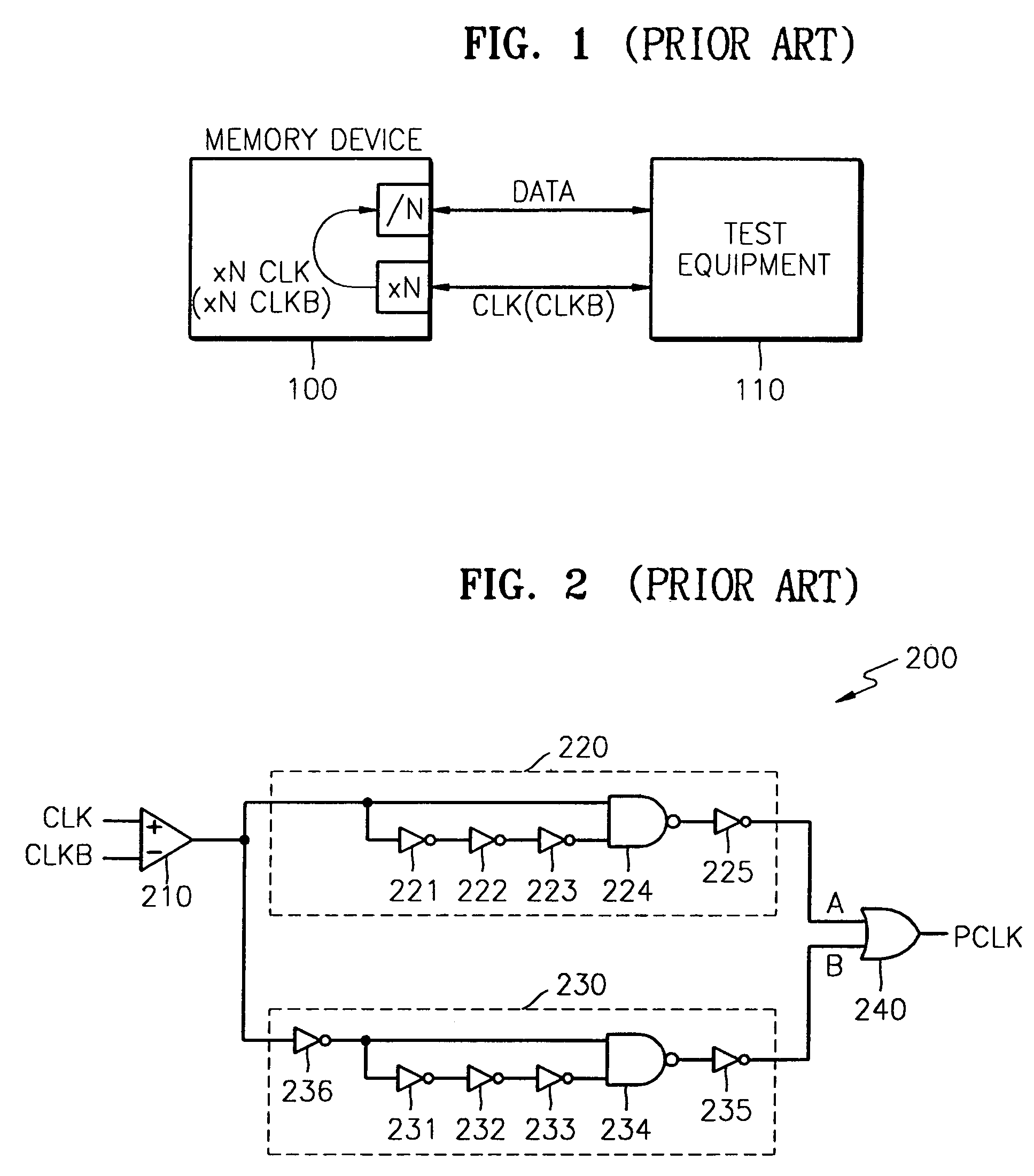
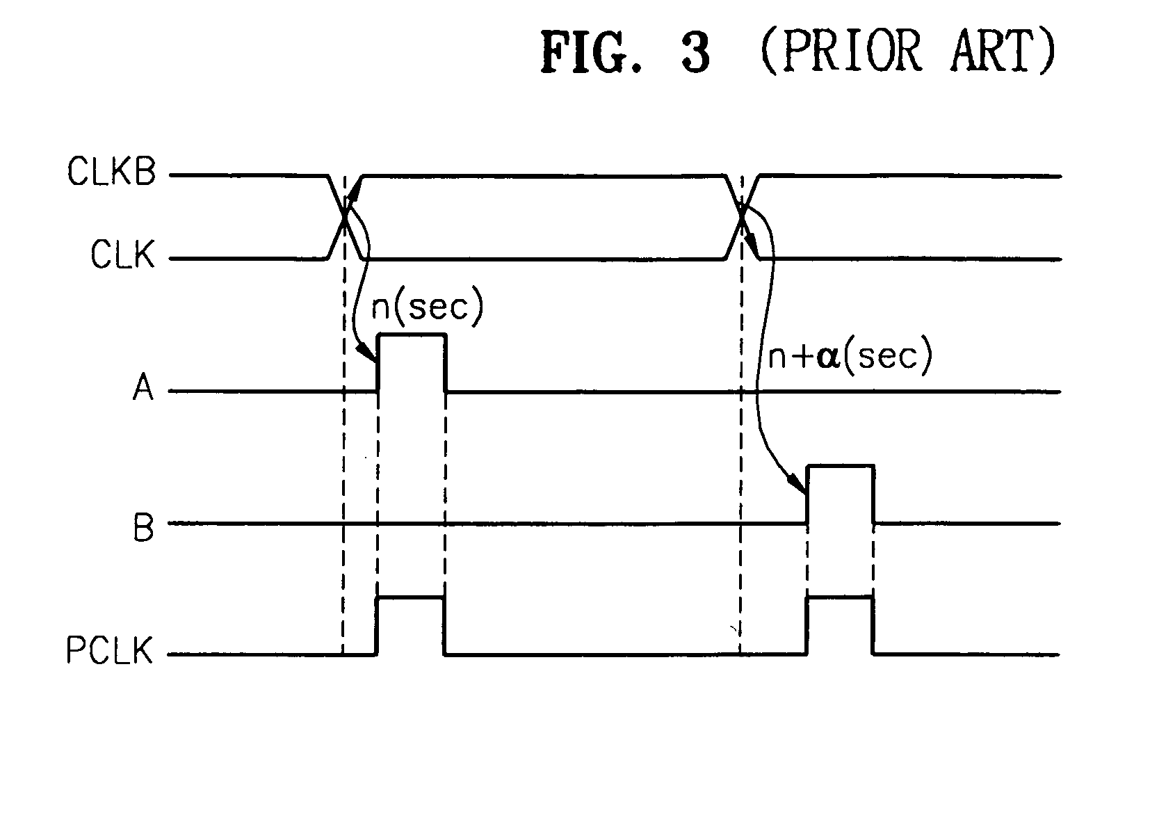
[0039]FIG. 1 is a schematic view of a semiconductor device and test equipment. As shown in FIG. 1, a semiconductor memory device 100 interfaces with test equipment 110 in order to test the semiconductor device 100. However, the operating speeds of the semiconductor device 100 and the test equipment 110 are different from each other.

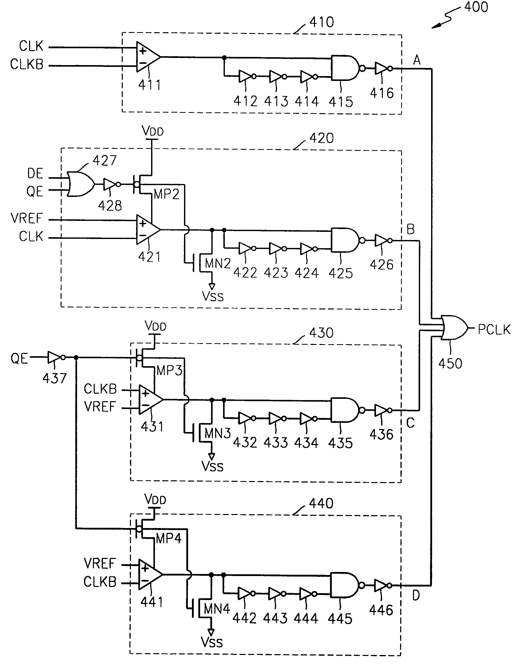
[0040]Thus, in the present invention, there is provided a frequency multiplier which receives external clock signals CLK and CLKB input from the test equipment 110 and multiplies the frequencies of the external clock signals CLK and CLKB by N times and a data output buffer which outputs data so as to interface data output from an output terminal of the semiconductor device 100 with the test equipment 110.

[00...


PUM


Abstract

In a frequency multiplier and a method of multiplying a frequency of an external clock signal, a data output buffer, and a semiconductor device including the frequency multiplier and the data output buffer, the frequency multiplier receives an external clock signal having a predetermined frequency and outputs an internal clock signal having greater frequency than the predetermined frequency. In the semiconductor device, the data output buffer outputs data tested in response to test data. Therefore, it is possible to test a plurality of memory cells at a time by using a clock signal having a low frequency. In addition, the time and cost required for the test can be greatly reduced, and conventional testing equipment that operates at a relatively low frequency can be effectively used.

Description

BACKGROUND OF THE INVENTION[0001]This application claims priority from Korean Patent Application No. 2002-59831, filed on Oct. 1, 2002, in the Korean Intellectual Property Office, the disclosure of which is incorporated herein in its entirety by reference.[0002]1. Field of the Invention[0003]The present invention relates to a semiconductor device, and more particularly to a frequency multiplier and a method of multiplying the frequency of an external clock signal, a data output buffer, and a semiconductor device including the frequency multiplier and the data output buffer.[0004]2. Description of the Related Art[0005]In a process of designing a semiconductor device, a memory chip is tested to determine whether any of its memory cells have defects, following its fabrication. Memory chip tests can be performed during the semiconductor manufacturing process and / or after the memory chip is manufactured to check for normal operation.[0006]In the test that is performed following manufactu...

Claims


Application Information

Patent Timeline
Patent Type & Authority Patents(United States)
IPC IPC(8): G11C11/40G06F1/04G11C29/00G11C29/12H03B1/00H03B19/00H03B19/10H03K5/00H03K5/1534H03K21/10
CPCH03K5/00006H03K5/1534G11C11/40
Inventor KWON, KYOUNG-HWANJANG, HYUN-SOONKIM, KYU-HYOUN
Owner SAMSUNG ELECTRONICS CO LTD
Why Eureka
Try Eureka