Semiconductor device for domain crossing

a semiconductor and domain technology, applied in the field of semiconductor devices, can solve the problems of unstable flip-flop delaying dll clock, low power voltage, and inability to operate the high-frequency semiconductor system properly,

Inactive Publication Date: 2005-12-27
SK HYNIX INC
View PDF16 Cites 57 Cited by
  • Summary
  • Abstract
  • Description
  • Claims
  • Application Information

AI Technical Summary

Benefits of technology

[0030]It is, therefore, an object of the present invention to provide a semiconductor system having a domain crossing circuit which detects a phase difference between an internal clock and a delay locked loop (DLL) clock, senses a flight time when the DLL clock passes from a DLL clock g...

Problems solved by technology

However, if an operation of the semiconductor system is faster, the plurality of flip-flops delaying DLL clock is unstable because a setup time of each flip-flop is not guaranteed.
In addition, an abnormal operation of the semiconductor system can resu...

Method used


Image

  • Semiconductor device for domain crossing
  • Semiconductor device for domain crossing
  • Semiconductor device for domain crossing

Examples


Embodiment Construction

[0054]Hereinafter, a semiconductor device for domain crossing according to the present invention will be described in detail referring to the accompanying drawings.

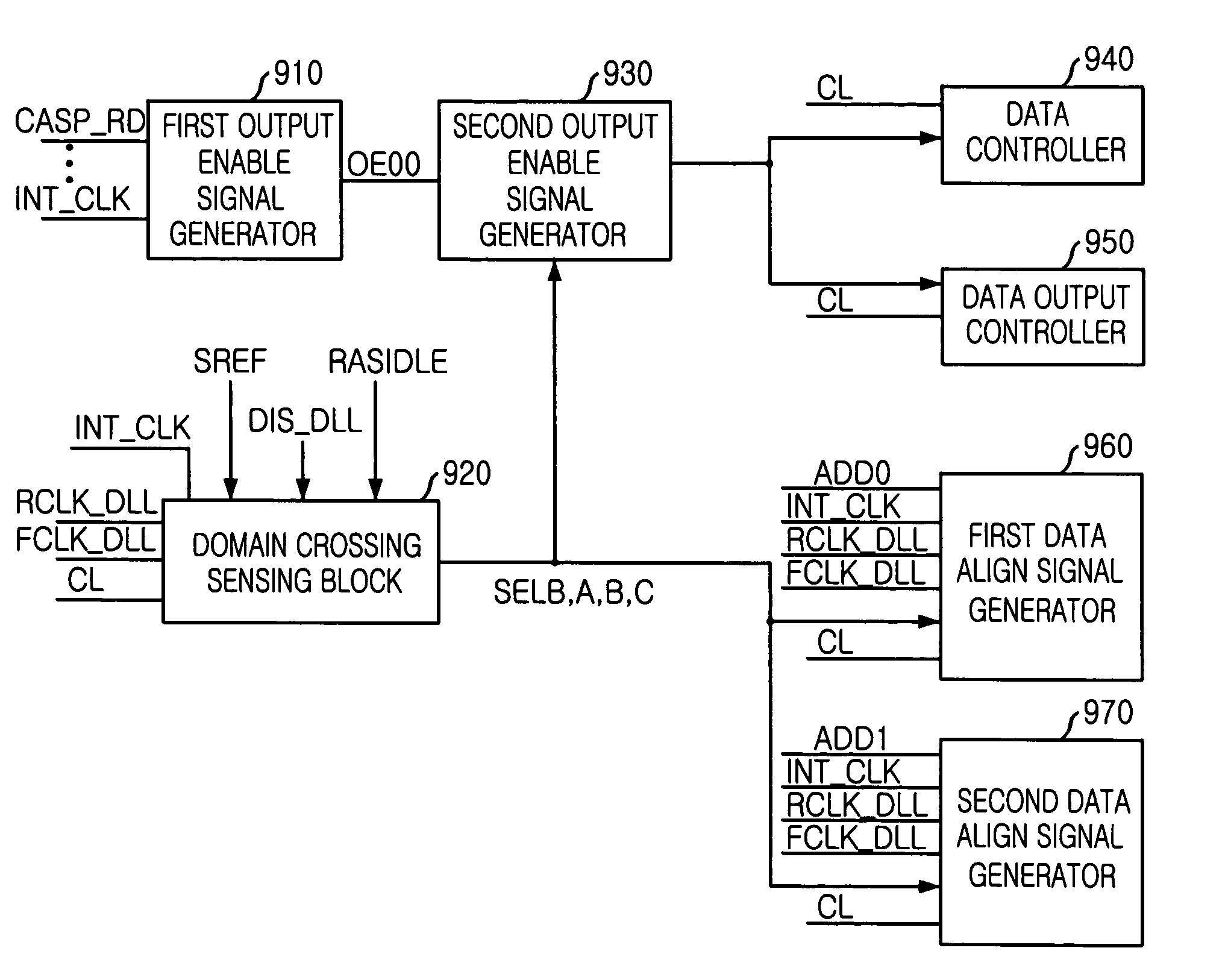
[0055]FIG. 9 is a block diagram describing a domain crossing circuit in accordance with the present invention.

[0056]The domain crossing circuit includes a domain crossing sensing block 920, a first output enable signal generator 910, a second output enable signal generator 930, a data controller 940, a data output controller 950, a first data align signal generator 960 and a second data align signal generator 970.

[0057]The domain crossing sensing block 920 enabled by an internal clock INT—CLK receives a refresh state signal SREF, a DLL disable signal DIS—DLL and a RAS idle signal RASIDLE. Then, the domain crossing sensing block 920 detects a phase of rising and falling DLL clock signals RCLK—DLL and FCLK—DLL in response to a CAS latency CL and generates a setup selection signal SELB and a plurality of output selection sig...


PUM


Abstract

An apparatus, for use in a semiconductor device, for providing a domain crossing operation. The apparatus includes a domain crossing sensing block, in response to an operation mode signal, first and second delay locked loop (DLL) clock signals and a CAS latency, generates a plurality of selection signals. An output enable signal generator, in response to the plurality of selection signals, generates a plurality of output enable signals. A data control block, in response to the output enable signals and the CAS latency, controls a data output operation in the semiconductor device. Each of a plurality of data align block, in response to the selection signals, the first and second DLL clock signals and an address signal, aligns data corresponding to the address signal in the data output operation.

Description

FIELD OF INVENTION[0001]The present invention relates to a semiconductor device; and, more particularly, to a semiconductor device for domain crossing in a synchronous dynamic random access memory SDRAM and double data rate DDR, DDRII, DDRIII SDRAMs.DESCRIPTION OF PRIOR ART[0002]Generally, in a semiconductor memory device, a domain crossing takes place during its operation. For instance, some devices use an internal clock as an operation reference and the others use a delay locked loop (DLL) clock as the operation reference. In addition, a conversion from a receiver domain to a transmitter domain comes under the domain crossing.[0003]FIG. 1 is a block diagram showing a semiconductor device included in a conventional memory device for domain crossing.[0004]As shown, the conventional memory device includes a first flip-flop 131, a memory cell 140, a second flip-flop 150, a plurality of pipe latches 180, a driver 190, a third flip-flop 132, a domain crossing circuit 161, a controlling ...

Claims


Application Information

Patent Timeline
IPC IPC(8): G11C11/407G11C7/10G11C7/22G11C8/00G11C11/40G11C11/4063G11C11/4076G11C11/4093G11C11/4096
CPCG11C7/1039G11C7/1051G11C7/106G11C7/1066G11C7/1069G11C7/22G11C7/222G11C11/4076G11C11/4096G11C7/1072G11C2207/2281G11C11/40
Inventor PARK, NAK-KYU
Owner SK HYNIX INC
Why Eureka
Try Eureka