

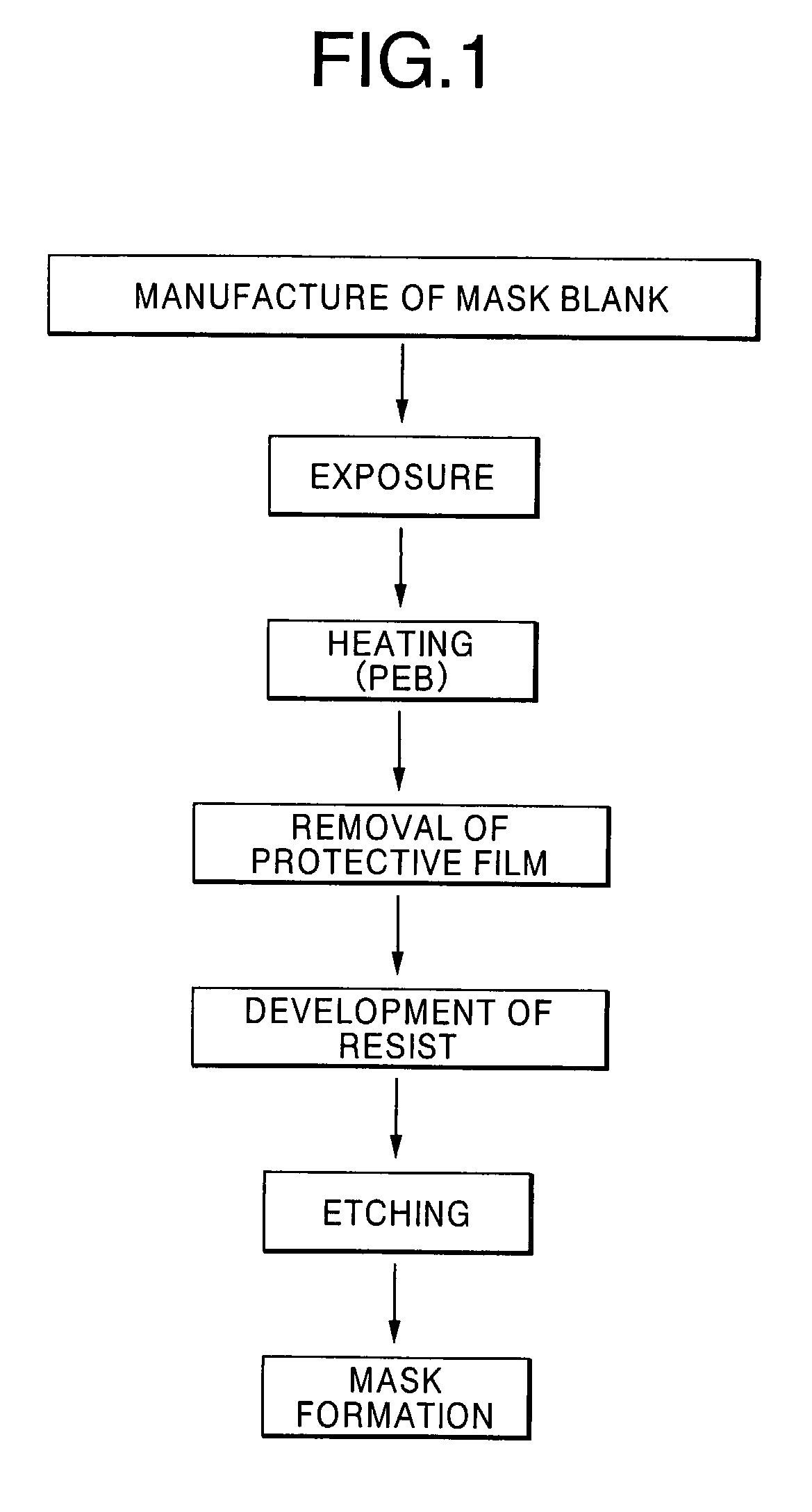
Method of patterning a mask blank
a mask and patterning technology, applied in the field of mask blanks, can solve the problems of long time to write traces, reduce the productivity of the mask, and take about 6 to 40 hours, and achieve the effects of improving the uniformity of the applied chemically, high precision and stable patterning, and satisfactory dimensional precision
- Summary
- Abstract
- Description
- Claims
- Application Information
AI Technical Summary
Benefits of technology
Problems solved by technology
Method used
Image

Examples
example 1
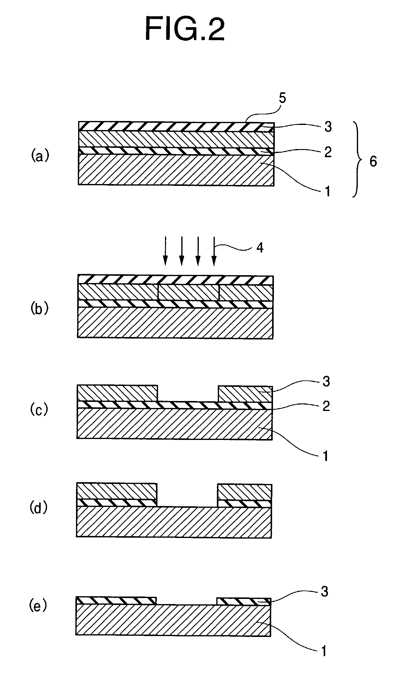
[0069]A film of a chemically amplified resist (available from FUJIFILM Arch Co., Ltd. under the trade name of FEP-171) was applied to a thickness of 0.4 μm onto a 6-inch square quartz substrate carrying a chromium film formed thereon, was dried on a hot plate at 110° C. for 10 minutes and thereby yielded a chemically amplified resist film.
[0070]Separately, 95 parts by weight of poly(α-methylstyrene) (available from Aldrich, number average molecular weight: 4000) and 5 parts by weight of bis(tert-butylphenyl)iodonium nonafluorobutanesulfonate were dissolved in cumene and thereby yielded a solution. A film of the solution as a photosensitive protective film according to the present invention was then applied onto the chemically amplified resist film to a thickness of 0.1 μm and thereby yielded a mask blank.
[0071]Next, traces ranging from 1.0 μm to 0.2 μm were patterned on the mask blank using an electron beam exposure system (available from JEOL Ltd. under the trade name of JBX-6000 F...
example 2
[0073]A mask blank was manufactured in the same manner as in Example 1.
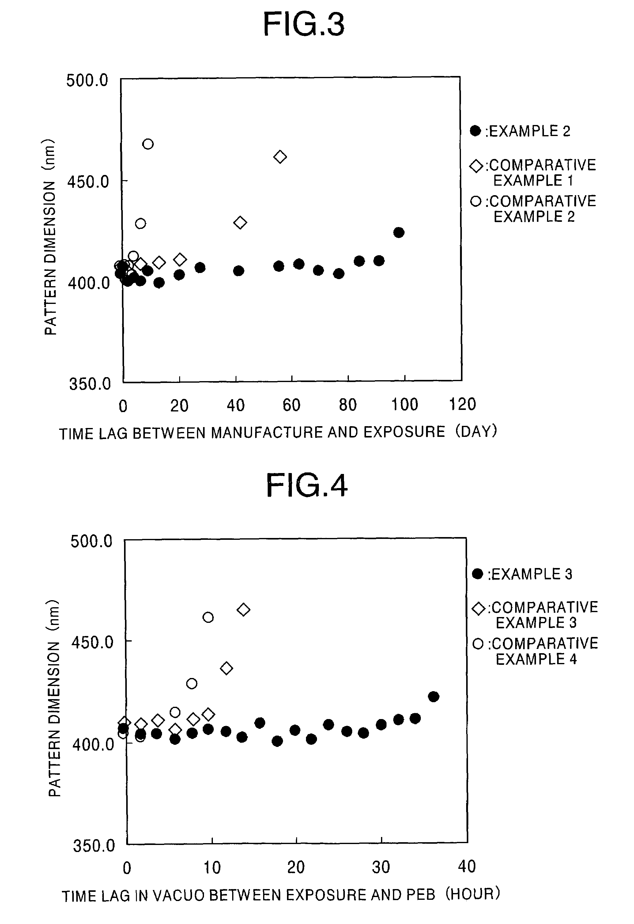
[0074]The mask blank was patterned to a size of 400 nm in the same manner as in Example 1, except the following procedure. Specifically, in Example 1, the mask blank was exposed to electron beams and thereby patterned immediately after its manufacture. However, in Example 2, the time lag between manufacture and exposure of the mask blank, i.e., the time period between the step of FIG. 2A and the step of FIG. 2B, was varied. During this time period, the mask blank was left in the air.
example 3
[0084]A mask blank was manufactured in the same manner as in Example 1. Subsequently, the mask blank was irradiated with electron beams to thereby pattern to a size of 400 nm in the same manner as in Example 1, except the following procedure. Specifically, in Example 1, the mask blank was heated immediately after its exposure to electron beams. However, in Example 3, the time lag between exposure and heating of the mask blank (post exposure baking, PEB) was varied. During this time period, the mask blank was left in an electron beam exposure system. Specifically, Example 3 was performed to verify the relationship between the stability in resist pattern dimension and the time lag between exposure to electron beams and heat treatment (post exposure baking) of the mask blank when the mask blank was left in vacuo.
PUM
| Property | Measurement | Unit |
|---|---|---|
| thickness | aaaaa | aaaaa |
| thickness | aaaaa | aaaaa |
| accelerating voltage | aaaaa | aaaaa |
Abstract
Description
Claims
Application Information